Original Link: https://www.anandtech.com/show/5067/understanding-tlc-nand
Understanding TLC NAND
by Kristian Vättö on February 23, 2012 1:14 PM EST- Posted in
- Storage
- SSDs
- OCZ
- Indilinx Everest
- TLC
A Brief Introduction to SSDs and Flash Memory
In almost every SSD review we have published, Anand has mentioned how an SSD is the biggest performance upgrade you can make today. Why would anyone use regular hard drives then? There is one big reason: price. SSD prices are still up in the clouds when compared to hard drive prices (especially before the Thailand floods) so for many, SSDs have not been a realistic option.
Forking over $700 for a 512GB SSD sounds crazy because a 500GB hard drive can be had for less than $50. Smaller capacities like 64GB and 128GB can already be bought for around $100 and $200 respectively, but unless you have the ability to have an SSD plus hard drive combo, such a small SSD doesn't usually cut it. If you have a desktop, the SSD + HDD combo should not be a problem but many laptops only have space for one 2.5" drive (unless you are willing to mod it afterwards by replacing the optical drive). SSD prices have been dropping for years now, but if the current rate continues it will take years before a $399 Walmart PC includes a reasonable size SSD. So what can be done?
Most of the time, SSD production costs are cut by shrinking the NAND die. Shrinking the die is the same as with CPUs: you move to a smaller manufacturing process, e.g. from 34nm to 25nm. In flash memory, this means you can increase the density per die and usually the physical die size is also smaller, meaning more dies from a single wafer. A die shrink is an effective way to lower costs but moving from one process to another takes time and the initial ramp of the new flash isn't necessarily cheaper. Once the new process has matured and supply has met demand, prices start to fall.
Since die shrinks are a relatively slow way to lower SSD prices and only contribute to steady reduction of prices, anyone looking to push higher capacity SSDs into the mainstream today will need something more. Right now, that "something more" is called Triple Level Cell flash, commonly abbreviated as TLC.

Rather than shrinking the die to improve density/capacity, TLC (like MLC) increases the number of bits per cell. In our SSD Anthology article, Anand described how SLC and MLC flash work, and TLC works the same way but takes things a step further. Normally, you apply a voltage to a cell and keep increasing it until you reach a point where the result is far enough from the "off" state that you now consider the cell as being "on". This is how SLC works, storing one bit per cell. For MLC, you store two bits per cell, which means instead of two voltage states (0 and 1) you have four states (00, 01, 10, 11). TLC takes that a step further and stores three bits per cell, or eight voltage states (000, 001, 010, 011, 100, 101, 110, and 111). We will take a deeper look into voltage states and how they work in the next page.
Even though SLC, MLC and TLC operate the same way, there is one crucial difference. Lets take a look at what happens to a NAND array depending on the amount of data per cell. The image above is a NAND array with ~16 billion transistors (one transistor is required per cell), i.e. 16 gigabits (Gb). This array can be turned into either SLC, MLC, or TLC. The actual array and transistors are equivalent in all three flash types; there is no physical difference. In the case of SLC flash, only one bit of data will be stored in one cell, hence your final product has a 16Gb capacity. When you up the bits per cell to two (MLC), you get 32Gb because now you have two bits per cell and there are still 16 billion cells. Likewise, three bits per cell (TLC) yields 48Gb.
However, TLC is a horse of slightly different color in this case. Capacities usually go in powers of two (2, 4, 8, 16 and so on) and 48 is not a power of two. To get a number that is a power of two, the original NAND array is chopped down. In our example, the array must be 10.67Gb in order to be 32Gb with three bits per cell, but since that is the same capacity as an MLC die, what is the benefit? You don't get more storage per die, but the actual die is smaller because the original 16Gb array has been reduced to a 10.7Gb array. That means more dies per wafer and hence lower cost.
| Comparison of NAND Wholesale Prices | |||
| Cell Type | SLC | MLC | TLC |
| Price per GB | $3.00 | $0.90 |
$0.60 |
Prices provided by OCZ
The theoretical price advantage of TLC isn't as great as SLC versus MLC, but it's still significant. In percentage, that is over a 30% reduction. The main reason is that MLC provides twice the capacity when compared to SLC (2bits per cell versus 1bit per cell), whereas TLC provides only 50% more than MLC (3bits per cell versus 2bits per cell). In fact, the price difference between MLC and TLC is directly proportional. TLC die is 33% smaller than a similar MLC die and in the prices provided by OCZ, TLC is also 33% cheaper than MLC. In theory, SLC should follow this equation as well and be priced at $1.80/GB, but there's limited 2Xnm SLC out in the wild, making SLC significantly more expensive than MLC and TLC at this point.
The reality of the matter is a little less clear. TLC NAND today isn't all that much cheaper than MLC NAND, which has contributed to its relative absence in the consumer SSD space. There's also a lack of controller support and market interest, which contribute to the higher prices of course.
Weaknesses of TLC: One Degree Worse than MLC
In a perfect world, increasing the number of bits per cell sounds like a very easy way to increase capacities while keeping the prices down. So, why not put a thousand bits inside every cell? Unfortunately, there's a downside to storing more bits per cell.
Fundamentally, TLC shares the same problems as MLC when compared to SLC, but takes things one step further. Now that there are eight voltage levels to check, random reads will take more time: 100µs for TLC. That's four times longer than what it takes SLC to random read one bit, and twice as long as what it takes for MLC to complete the same task. Programming will also take longer, but unfortunately we don't have any figures for TLC yet.
| SLC | MLC | TLC | |
| Bits per Cell | 1 | 2 | 3 |
| Random Read | 25 µs | 50 µs | 100 µs |
| Erase | 2ms per block | 2ms per block | ? |
| Programming | 250 µs | 900 µs | ? |
On top of the decrease in performance, TLC also has worse endurance than MLC and SLC. Precise P/E cycle figures are not yet known, but we are most likely looking at around 1000 cycles. Hynix has a brief product sheet for their 48nm TLC flash, which has 2500 P/E cycles. At least in MLC flash, the move to 3Xnm halved the P/E cycles so we would be looking at 1250 cycles. 2Xnm brought even fewer cycles, roughly 3,000, and with same math we get 750 cycles for 2Xnm TLC. X-bit labs reported 1,000 cycles for TLC, which sounds fair. It's also good to keep in mind that endurance can vary depending on the manufacturer and maturity of the process. For example the first 25nm NANDs were good for only ~1,000 cycles, whereas today's chips should last for over 3,000 cycles.
| 5Xnm | 3Xnm | 2Xnm | |
| SLC | 100,000 |
100,000 |
N/A |
| MLC | 10,000 | 5,000 | 3,000 |
| TLC | 2,500 | 1,250 |
750 |
But why does NAND with more bits degrade quicker? The reason lies in the physics of silicon. To understand this, we need to take a look at our beloved Mr. N-channel MOSFET again.
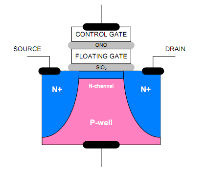
When you program a cell, you are placing a voltage on the control gate, while source and drain regions are held at 0V. The voltage forms an electric field, which allows electrons to tunnel through the silicon oxide barrier from the N-channel to the floating gate. This process is called tunneling. The silicon oxide acts as an insulator and will not allow electrons to enter or escape the floating gate unless an electrical field is formed. To erase a cell, you apply voltage on the silicon substrate (P-well in the picture) and keep control gate voltage at zero. An electric field will be formed which allows the electrons to get through the silicon oxide barrier. This is why NAND flash needs to be erased before it can be re-programmed: you need to get rid of the old electrons (i.e. old data) before you can apply new electrons (i.e. new data).
But what does this have to do with SLC, MLC and TLC? The actual MOSFET is exactly the same in all three cases, but take a look at the table below.
| SLC | "0" | High Voltage |
| "1" | Low Voltage | |
| MLC | "00" | High Voltage |
| "01" | Med-High Voltage | |
| "10" | Med-Low Voltage | |
| "11" | Low Voltage | |
| TLC | "000" | Highest Voltage |
| "001" | High Voltage | |
| "010" | Med-High Voltage | |
| "100" | High-Medium Voltage | |
| "011" | Low-Medium Voltage | |
| "101" | Med-Low Voltage | |
| "110" | Low Voltage | |
| "111" | Lowest Voltage |
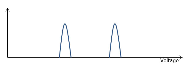
SLC
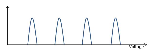
MLC
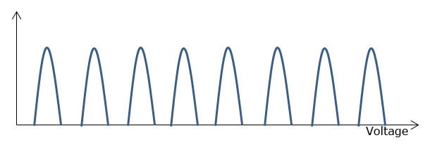
TLC
SLC only has two program states, "0" and "1". Hence either a high or low voltage is required. When the amount of bits goes up, you need more voltage stages. With MLC, there are four states, and eight states with TLC. The problem is that the silicon oxide layer is only about 10nm thick and it's not immortal; it wears out every time it's used in the tunneling process. When the silicon oxide layer wears out, the atomic bonds break and during the tunneling process, some electrons may get trapped inside the silicon oxide. This builds up negative charge in the silicon oxide, which negates some of the the control gate voltage.
At first, erasing becomes slower because higher voltages need to be applied (and for a longer time) before the right voltage is found. Higher voltage causes more stress on the oxide, wearing it out even more. Eventually, erasing will take so long that the block has to be retired to maintain the performance. There is a side effect, though. Programming will be faster because there is already some voltage in the cell due to the electron trapping. However, the time won because of that is much smaller than the time it takes to erase the cell when more voltage pulses are required to erase the cell. That's why the block has to be retired when the wear level reaches a certain point.
Here comes the differerence between SLC, MLC and TLC. The fewer bits you have per cell, the more voltage room you have. In other words, SLC can tolerate more changes in the voltage states because it has only two states. In TLC, there are eight, so the margin for errors is a lot smaller.
Lets assume that we have an SLC NAND that takes voltage between 0V and 14V. To program the cell to "1", a voltage between 4V and 5V needs to be applied. Likewise, you need a voltage from 9V to 10V to program the cell to "0". In this scenario, there is 4V of "spare" voltage between the states. If we apply this example to MLC NAND, the spare voltage will be cut to half, 2V. With TLC, that spare value is only 0.67V if we use the same 1V per voltage state ideaology.
However, when the oxide wears out and a higher voltage is needed, the programming voltages go up. To use the SLC example above, you would now need a voltage between 4V and 6V to program the cell to "0". That means a 1V loss in the spare voltage. And here comes the difference. Since SLC has more spare voltage between the states, it can tolerate a higher voltage change until the erase will be so slow that the block needs to be retired. This is why SLC has a substantially higher P/E cycle count; you can erase and reprogram the cell more times. Likewise, TLC tolerates the least change in voltage states, so it has the lowest amount of P/E cycles.
Availability and Controller support
Just to make this clear, TLC isn't anything new. For example Hynix had a 32Gb 48nm TLC die in 2008. This is because TLC was originally used for devices like USB flash drives, where its poor endurance would be negligible. Most SSD OEMs have been toying with TLC SSDs for at least a year now but we haven't seen any commercial products. OCZ had originally planned to introduce its first TLC based SSD in the Q1 2012, however TLC pricing simply hasn't made sense yet. Unless OCZ can leverage a significant cost savings over 2-bit-per-cell MLC, the added headaches of bringing a lower performing TLC part to market don't make sense.
However there's still significant motivation to migrate towards TLC NAND. Further bringing down costs, particularly for consumer SSDs aimed at light, particularly read heavy workloads makes a lot of sense. Increasing pressure from Intel to deliver cheaper SSD enabled Ultrabooks, and Apple's desire to move all mainstream Macs to solid state storage are two major motivations. MLC NAND pricing will eventually get low enough to meet these (and more) needs, but TLC definitely accelerates the process.
TLC does require controller and firmware support. In the client SSD space only OCZ has been aggressive with announcing that its Indilinx Everest controller supports 3-bit-per-cell NAND.
Adding controller support for an extra bit per cell is more than just updating the datasheet and claiming it works. The ECC engine needs to be updated as the controller will face more frequent and more severe errors with TLC NAND (and its associated lower endurance rating).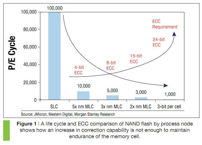
Maintaining low write amplification is even more important with TLC NAND. With significantly fewer available program/erase cycles, burning through them due to high write amplification isn't acceptible. While NAND endurance isn't really an issue for most client MLC drives, it may be an issue for TLC based drives.
Our thoughts are a bit mixed. On the one hand, cheaper SSDs are exactly what consumers want. The performance is still there compared to hard drives, no matter what NAND is used. If you go to an Apple Store today and try out MacBook Air and Mac Pro, the MacBook Air will often feel faster, even though it's the slower Mac in terms of processing power. This is solely due to the presence of an SSD. An SSD can bring new life to a computer that is otherwise considered obsolete. That's why we think everyone would want an SSD, but it's understandable that the masses won't adopt SSDs until the price and capacities are reasonable. This is definitely where TLC shines—it provides us with noticeably cheaper SSDs, possibly cheap enough for the masses to adopt (e.g. well under $1 per GB).
On the other hand, we're concerned that the cut in prices is done at the expense of endurance. One advantage often heard about buying an SSD is that SSDs are a lot more reliable than hard drives. In terms of P/E cycles, that is probably true with current MLC NAND. However, there have been quite a few widespread firmware issues, such as SF-2281 BSOD and Intel 320 Series 8MB bugs. Those have been fixed, and we may finally be looking at SSDs which have good performance, adequate endurance, and are more or less trouble-free. However, TLC will require new controller logic, and new logic may result in additional firmware issues.
The earliest SSDs lacked performance, even though they were faster than most hard drives, especially in seek times. In just a few years, performance has increased exponentially, maybe even to a point where the average user won't notice the difference between the fastest SSD and a mediocre SSD.
Given the desire for performance, reliability, and cost, TLC NAND may take away one from the triplet: endurance. Notice we said "may", because P/E cycles aren't everything. It has been claimed that algorithms to minimize write amplification will follow Moore's Law, just like NAND does. In other words, every time there is a die shrink, wear leveling has been improved in order to keep endurance the same. On top of that, improvements in manufacturing technologies can keep the P/E count up as well. 20nm IMFT MLC is claimed to have 3000-5000 P/E cycles, just like 25nm IMFT MLC.
The good news is, MLC NAND will stay in production and hence MLC NAND based SSDs are not going anywhere. What TLC will provide is freedom of choice. If you use your computer for checking email and browsing the Internet, no doubt a TLC based SSD will be sufficient. For the majority of consumers, TLC SSDs should meet their demands.
In addition, the SSD market is evolving quickly; if you buy the best SSD today, it won't be the best for very long. Let's say that it lasts you for four years. In that time, the SSD market will change a lot—four years ago, we were looking at 16GB SSDs for nearly $600! By the time a typical SSD is ready for replacement, you will be looking at much faster SSD with more capacity, and likely for a lower price. In 4.5 years, we have gone from that 16GB offering with performance that often trailed behind contemporary HDDs to 120GB SSDs that are up to a couple orders of magnitude faster than HDDs on random access patterns (and still several times faster for sequential tranfers), all for a starting price of around $170. If that pattern holds for the next four years, we'll be looking at ~1TB SSDs in four years that offer transfer rates that would saturate multi-lane PCIe interfaces at even lower prices. While we expect the rate of progress to be quite a bit slower over the next four years, there's still plenty of room for improvements in SSD technology.
As far as TLC-based SSDs are concerned, all we can do now is to wait for the first product announcements to come. Once we get some review samples, we'll be sure to put them through our SSD test suite and see how they stack up to existing drives.


