Original Link: https://www.anandtech.com/show/9390/the-amd-radeon-r9-fury-x-review
The AMD Radeon R9 Fury X Review: Aiming For the Top
by Ryan Smith on July 2, 2015 11:15 AM EST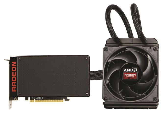
Almost 7 years ago to this day, AMD formally announced their “small die strategy.” Embarked upon in the aftermath of the company’s struggles with the Radeon HD 2900 XT, AMD opted against continuing to try beat NVIDIA at their own game. Rather than chase NVIDIA to absurd die sizes and the risks that come with it, the company would focus on smaller GPUs for the larger sub-$300 market. Meanwhile to compete in the high-end markets, AMD would instead turn to multi-GPU technology – CrossFire – to offer even better performance at a total cost competitive with NVIDIA’s flagship cards.
AMD’s early efforts were highly successful; though they couldn’t take the crown from NVIDIA, products like the Radeon HD 4870 and Radeon HD 5870 were massive spoilers, offering a great deal of NVIDIA’s flagship performance with smaller GPUs, manufactured at a lower cost, and drawing less power. Officially the small die strategy was put to rest earlier this decade, however even informally this strategy has continued to guide AMD GPU designs for quite some time. At 438mm2, Hawaii was AMD’s largest die as of 2013, still more than 100mm2 smaller than NVIDIA’s flagship GK110.
AMD's 2013 Flagship: Radeon R9 290X, Powered By Hawaii
Catching up to the present, this month marks an important occasion for AMD with the launch of their new flagship GPU, Fiji, and the flagship video card based on it, the Radeon R9 Fury X. For AMD the launch of Fiji is not just another high-end GPU launch (their 3rd on the 28nm process), but it marks a significant shift for the company. Fiji is first and foremost a performance play, but it’s also new memory technology, new power optimization technologies, and more. In short it may be the last of the 28nm GPUs, but boy if it isn’t among the most important.
With the recent launch of the Fiji GPU I bring up the small die strategy not just because Fiji is anything but small – AMD has gone right to the reticle limit – but because it highlights how the GPU market has changed in the last seven years and how AMD has needed to respond. Since 2008 NVIDIA has continued to push big dies, but they’ve gotten smarter about it as well, producing increasingly efficient GPUs that have made it harder for a scrappy AMD to undercut NVIDIA. At the same time alternate frame rendering, the cornerstone of CrossFire and SLI, has become increasingly problematic as rendering techniques get less and less AFR-friendly, making dual GPU cards less viable than they once were. And finally, on the business side of matters, AMD’s market share of discrete GPUs is lower than it has been in over a decade, with AMD’s GPU plus APU sales now being estimated as being below just NVIDIA’s GPU sales.

AMD's Fiji GPU
Which is not to say I’m looking to paint a poor picture of the company – AMD Is nothing if not the perennial underdog who constantly manages to surprise us with what they can do with less – but this context is important in understanding why AMD is where they stand today, and why Fiji is in many ways such a monumental GPU for the company. The small die strategy is truly dead, and now AMD is gunning for NVIDIA’s flagship with the biggest, gamiest GPU they could possibly make. The goal? To recapture the performance crown that has been in NVIDIA’s hands for far too long, and to offer a flagship card of their own that doesn’t play second-fiddle to NVIDIA’s.
To get there AMD needs to face down several challenges. There is no getting around the fact that NVIDIA’s Maxwell 2 GPUs are very well done, very performant, and very efficient, and that between GM204 and GM200 AMD has their work cut out for them. Performance, power consumption, form factors; these all matter, and these are all issues that AMD is facing head-on with Fiji and the R9 Fury X.
At the same time however the playing field has never been more equal. We’re now in the 4th year of TSMC’s 28nm process and have a good chunk of another year left to go. AMD and NVIDIA have had an unprecedented amount of time to tweak their wares around what is now a very mature process, and that means that any kind of advantages for being a first-mover or being more aggressive are gone. As the end of the 28nm process’s reign at the top, NVIDIA and AMD now have to rely on their engineers and their architectures to see who can build the best GPU against the very limits of the 28nm process.
Overall, with GPU manufacturing technology having stagnated on the 28nm node, it’s very hard to talk about the GPU situation without talking about the manufacturing situation. For as much as the market situation has forced an evolution in AMD’s business practices, there is no escaping the fact that the current situation on the manufacturing process side has had an incredible, unprecedented effect on the evolution of discrete GPUs from a technology and architectural standpoint. So for AMD Fiji not only represents a shift towards large GPUs that can compete with NVIDIA’s best, but it represents the extensive efforts AMD has gone through to continue improving performance in the face of manufacturing limitations.
And with that we dive in to today’s review of the Radeon R9 Fury X. Launching this month is AMD’s new flagship card, backed by the full force of the Fiji GPU.
| AMD GPU Specification Comparison | ||||||
| AMD Radeon R9 Fury X | AMD Radeon R9 Fury | AMD Radeon R9 290X | AMD Radeon R9 290 | |||
| Stream Processors | 4096 | (Fewer) | 2816 | 2560 | ||
| Texture Units | 256 | (How much) | 176 | 160 | ||
| ROPs | 64 | (Depends) | 64 | 64 | ||
| Boost Clock | 1050MHz | (On Yields) | 1000MHz | 947MHz | ||
| Memory Clock | 1Gbps HBM | (Memory Too) | 5Gbps GDDR5 | 5Gbps GDDR5 | ||
| Memory Bus Width | 4096-bit | 4096-bit | 512-bit | 512-bit | ||
| VRAM | 4GB | 4GB | 4GB | 4GB | ||
| FP64 | 1/16 | 1/16 | 1/8 | 1/8 | ||
| TrueAudio | Y | Y | Y | Y | ||
| Transistor Count | 8.9B | 8.9B | 6.2B | 6.2B | ||
| Typical Board Power | 275W | (High) | 250W | 250W | ||
| Manufacturing Process | TSMC 28nm | TSMC 28nm | TSMC 28nm | TSMC 28nm | ||
| Architecture | GCN 1.2 | GCN 1.2 | GCN 1.1 | GCN 1.1 | ||
| GPU | Fiji | Fiji | Hawaii | Hawaii | ||
| Launch Date | 06/24/15 | 07/14/15 | 10/24/13 | 11/05/13 | ||
| Launch Price | $649 | $549 | $549 | $399 | ||
With 4096 SPs and coupled with the first implementation of High Bandwidth Memory, the R9 Fury X aims for the top. Over the coming pages we’ll get in to a deeper discussion on the architectural and other features found in the card, but the important point to take away right now it that it packs a lot of shaders, even more memory bandwidth, and is meant to offer AMD’s best performance yet. R9 Fury X will eventually be joined by 3 other Fiji-based parts in the coming months, but this month it’s all about AMD’s flagship card.
The R9 Fury X is launching at $649, which happens to be the same price as the card’s primary competition, the GeForce GTX 980 Ti. Launched at the end of May, the GTX 980 Ti is essentially a preemptive attack on the R9 Fury X from NVIDIA, offering performance close enough to NVIDIA’s GTX Titan X flagship that the difference is arguably immaterial. For AMD this means that while beating GTX Titan X would be nice, they really only need a win against the GTX 980 Ti, and as we’ll see the Fury X will make a good run at it, making this the closest AMD has come to an NVIDIA flagship card in quite some time.
Finally, from a market perspective, AMD will be going after a few different categories with the R9 Fury X. As competition for the GTX 980 Ti, AMD is focusing on 4K resolution gaming, based on a combination of the fact that 4K monitors are becoming increasingly affordable, 4K Freesync monitors are finally available, and relative to NVIDIA’s wares, AMD fares the best at 4K. Expect to see AMD also significantly play up the VR possibilities of the R9 Fury X, though the major VR headset, the Oculus Rift, won’t ship until Q1 of 2016. Finally, it has now been over three years since the launch of the original Radeon HD 7970, so for buyers looking for an update AMD’s first 28nm card, Fury X is in a good position to offer the kind of generational performance improvements that typically justify an upgrade.
Fiji’s Architecture: The Grandest of GCN 1.2
We’ll start off our in-depth look at the R9 Fury X with a look at the Fiji GPU underneath.
Like the Hawaii GPU before it, from a release standpoint Fiji is not really the pathfinder chip for its architecture, but rather it’s the largest version of it. Fiji itself is based on what we unofficially call Graphics Core Next 1.2 (aka GEN3), and ignoring HBM for the moment, Fiji incorporates a few smaller changes but otherwise remaining nearly identical to the previous GCN 1.2 chips. The pathfinder for GCN 1.2 in turn was Tonga, which was released back in September of 2014 as the Radeon R9 285.

So what does GCN 1.2 bring to the table over Hawaii and the other GCN 1.1 chips? Certainly the most well-known and marquee GCN 1.2 feature is AMD’s latest generation delta color compression technology. Tied in to Fiji’s ROPs, delta color compression augments AMD’s existing color compression capabilities with additional compression modes that are based around the patterns of pixels within a tile and the differences between them (i.e. the delta), increasing how frequently and by how much frame buffers (and RTs) can be compressed.
Frame buffer operations are among the most bandwidth intensive in a GPU – it’s a lot of pixels that need to be resolved and written to a buffer – so reducing the amount of memory bandwidth these operations draw on can significantly increase the effective memory bandwidth of a GPU. In AMD’s case, GCN 1.2’s delta color compression improvements are designed to deliver up to a 40% increase in memory bandwidth efficiency, with individual tiles being compressible at up to an 8:1 ratio. Overall, while the lossless nature of this compression means that the exact amount of compression taking place changes frame by frame, tile by tile, it is at the end of the day one of the most significant improvements to GCN 1.2. For Radeon R9 285 it allowed AMD to deliver similar memory performance on a 256-bit memory bus (33% smaller than R9 280’s), and for Fiji it goes hand-in-hand with HBM to give Fiji an immense amount of effective memory bandwidth to play with.
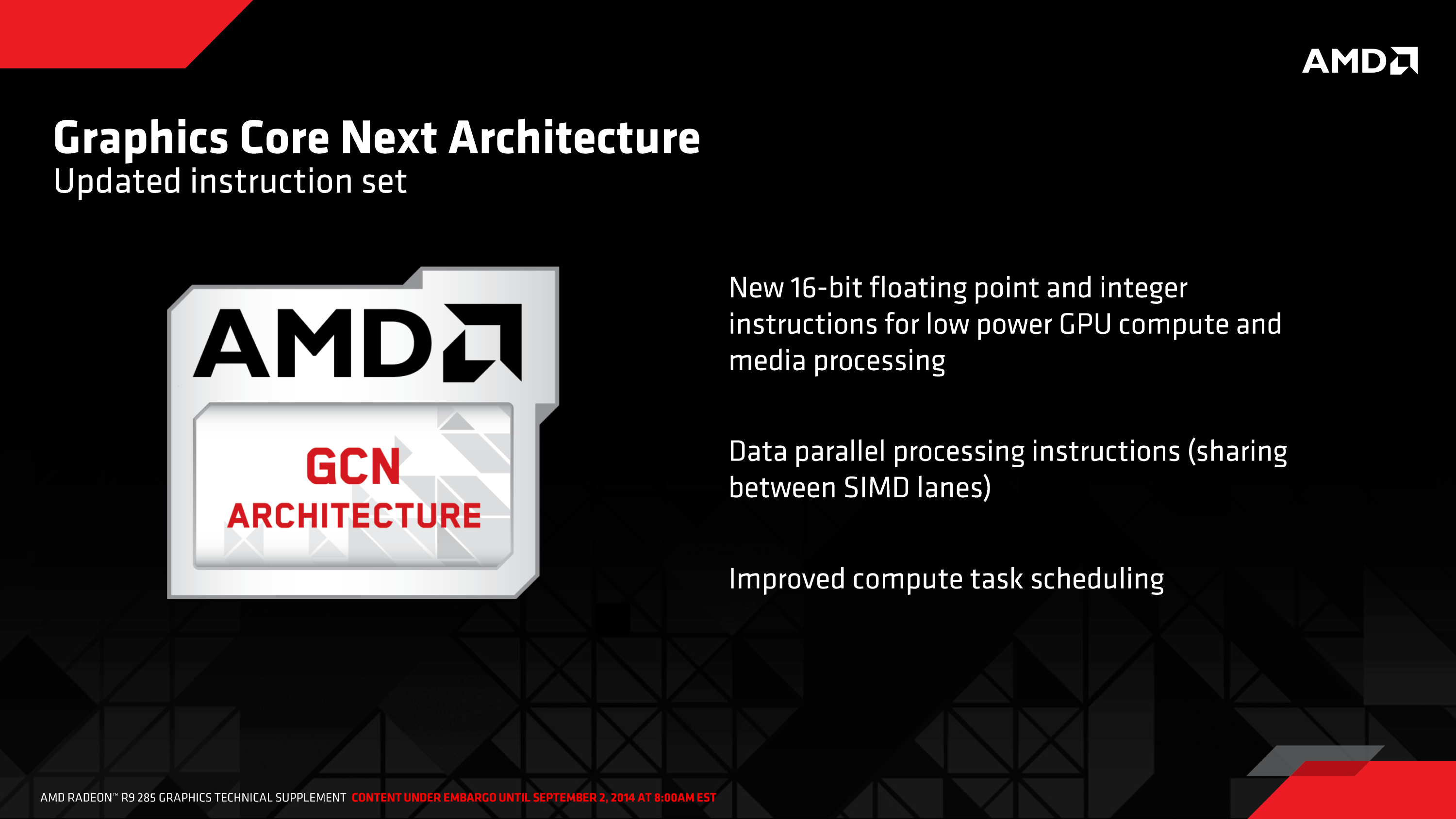
Moving on, AMD has also made some changes under the hood at the ALU/shader level for GCN 1.2. Many of these changes are primarily for AMD’s Carrizo APU, where task scheduling improvements go hand-in-hand with the AMD’s Heterogeneous System Architecture initiative and deliver improvements to allow the CPU and GPU to more easily deliver work to each other. Similarly, 16-bit instructions are intended to save on power consumption in mobile devices that use lower precision math for basic rendering.

More applicable to Fiji and its derivatives are the improvements to data-parallel processing. GCN 1.2 now has the ability for data to be shared between SIMD lanes in a limited fashion, beyond existing swizzling and other data organizations methods. This is one of those low-level tweaks I’m actually a bit surprised AMD even mentioned (though I’m glad they did) as it’s a little tweak that’s going to be very algorithm specific. For non-programmers there’s not much to see, but for programmers – particularly OpenCL programmers – this will enable newer, more efficient algorithms where when the nature of the work requires working with data in adjacent lanes.
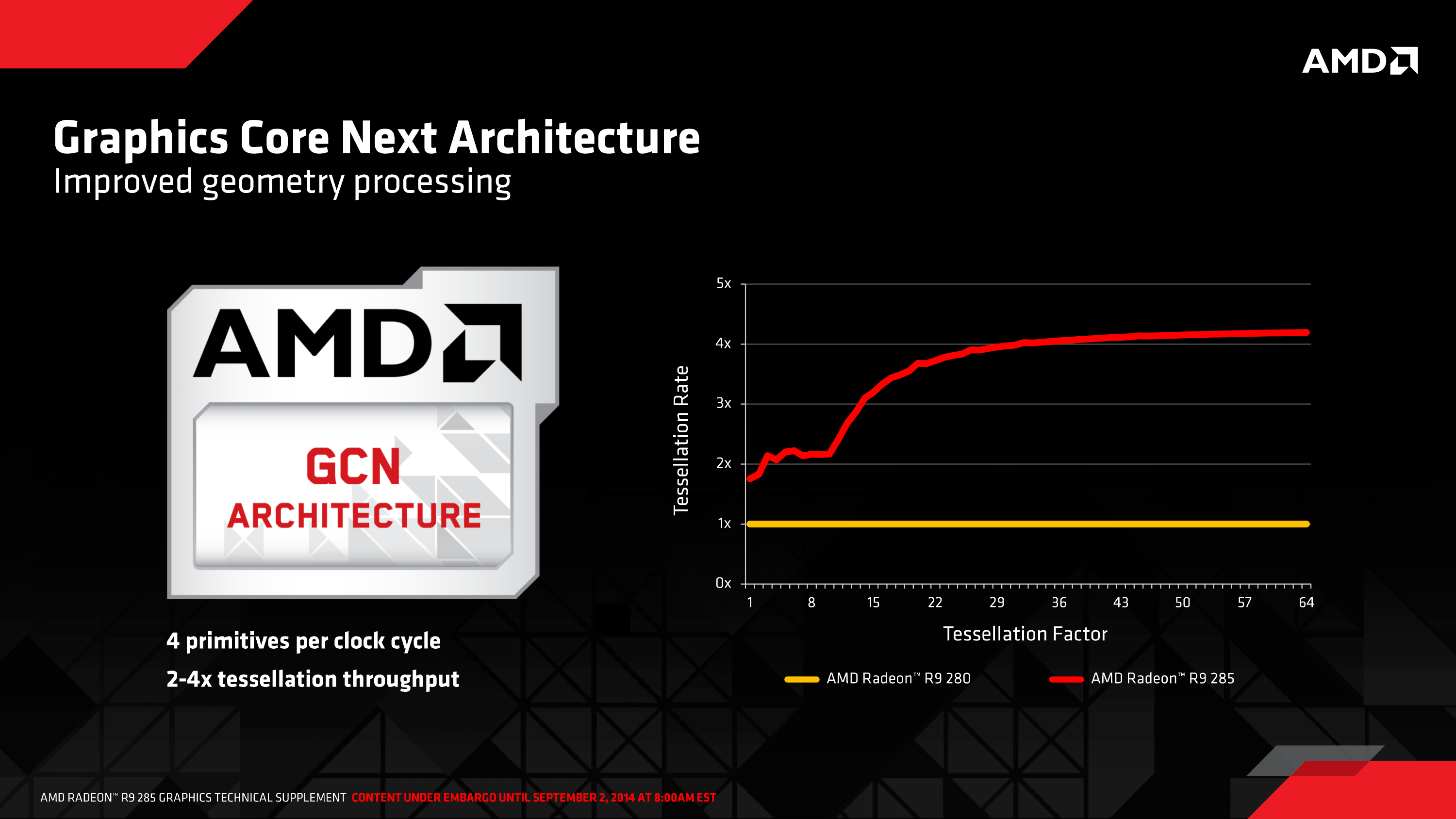
But for gamers, perhaps the most significant architectural improvement to GCN 1.2 and thereby Fiji are the changes made to tessellation and geometry processing. There is no single silver bullet here – after going with a 4-wide geometry front-end in Hawaii, AMD hasn’t changed it for Tonga or Fiji – but AMD has put in quite a bit of effort in to improving how geometry data moves around within the chip and how it’s used, on the basis that at this point the limitations aren’t in raw geometry performance, but rather the difficulties in achieving that performance.
Much of this effort has been invested in better handling small geometry, whether it’s large quantities of small batches, or even small quantities of small batches. The inclusion of small instance caching, for example, allows the GPU to better keep small batches of draw calls in cache, allowing them to be referenced and/or reused in the future without having to go to off-cache memory. Similarly, AMD can now store certain cases of vertex inputs for the geometry shader in shared memory, which like small instance caching allows for processing to take place more frequently on-chip, improving performance and cutting down on DRAM traffic.
More specific to Fiji’s incarnation of GCN is how distribution is handled. Load balancing and distribution among the geometry frontends is improved overall, including some low-level optimizations to how primitives generated from tessellation are distributed. Generally speaking distribution is a means to improve performance by removing bottlenecks, however AMD is now catching a specific edge case where small amplification factors don’t generate a lot of primitives, and in those cases they’re now skipping distribution since the gains are minimal, and more likely than not the cost from the bus traffic is greater than the benefits of distribution.
Finally, AMD has also expanded the vertex reuse window on GCN 1.2. As in the general case of reuse windows, the vertex reuse window is a cache of sorts for vertex data, allowing old results to be held in waiting in case they are needed again (as is often the cases in graphics). Though they aren’t telling us just how large the window now is, GCN 1.2 now features a larger window, which increases the hit rate for vertex data and as a result further edges geometry performance up since that data no longer needs to be regenerated.
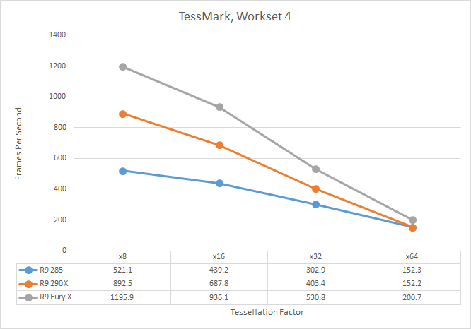
As with our R9 285 review, I took the time to quickly run TessMark across the x8/x16/x32/x64 tessellation factors just to see how tessellation and geometry performance scales on AMD’s cards as the tessellation factor increases. Keeping in mind that all of the parts here have a 4-wide geometry front-end, the R9 285, R9 290X, and R9 Fury X all have the same geometry throughput on paper, give or take 10% for clockspeeds. What we find is that Fury X shows significant performance improvements at all levels, beating not only the Hawaii based R9 290X, but even the Tonga based R9 285. Tessellation performance is consistently 33% ahead of the R9 290X, while against Tonga it’s anywhere between a 33% lead at high factors to a 130% lead at low tessellation factors, showing the influence of AMD’s changes to how tessellation is handled with low factors.
The Fiji GPU: Go Big or Go Home
Now that we’ve had a chance to take a look at the architecture backing Fiji, let’s talk about the Fiji GPU itself.
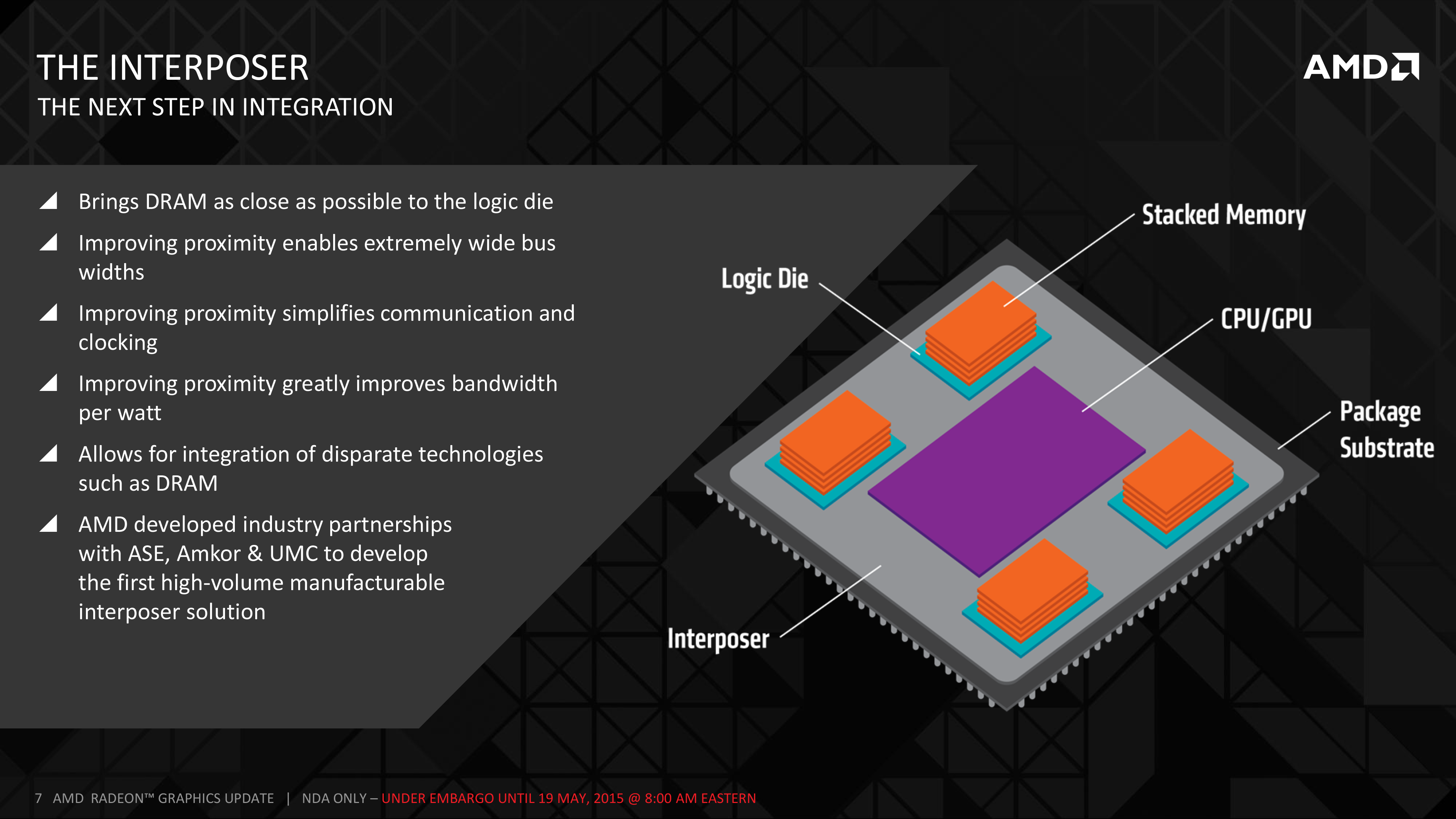
Fiji’s inclusion of High Bandwidth Memory (HBM) technology complicates the picture somewhat when talking about GPUs. Whereas past GPUs were defined by the GPU die itself and then the organic substrate package it sits on, the inclusion of HBM requires a third layer, the silicon interposer. The job of the interposer is to sit between the package and the GPU, serving as the layer that connects the on-package HBM memory stacks with the GPU. Essentially a very large chip without any expensive logic on it, the silicon interposer allows for finer, denser signal routing than organic packaging is capable of, making the ultra-wide 4096-bit HBM bus viable for the first time.

We’ll get to HBM in detail in a bit, but it’s important to call out the impact of HBM and the interposer early, since they have a distinct impact on how Fiji was designed and what its capabilities are.

As for Fiji itself, Fiji is unlike any GPU built before by AMD, and not only due to the use of HBM. More than anything else, it’s simply huge, 596mm2 to be precise. As we mentioned in our introduction, AMD has traditionally shied away from big chips, even after the “small die” era ended, and for good reason. Big chips are expensive to develop, expensive to produce, take longer to develop, and yield worse than small chips (this being especially the case early-on for 40nm). Altogether they’re riskier than smaller chips, and while there are times where they are necessary, AMD has never reached this point until now.
The end result is that for the first time since the unified shader era began, AMD has gone toe-to-toe with NVIDIA on die size. Fiji’s 596mm2 die size is just 5mm2 (<1%) smaller than NVIDIA’s GM200, and more notably still hits TSMC’s 28nm reticle limit. TSMC can’t build chips any bigger than this; Fiji is as big a chip as AMD can order.
| AMD Big GPUs | ||||
| Die Size | Native FP64 Rate | |||
| Fiji (GCN 1.2) | 596mm2 | 1/16 | ||
| Hawaii (GCN 1.1) | 438mm2 | 1/2 | ||
| Tahiti (GCN 1.0) | 352mm2 | 1/4 | ||
| Cayman (VLIW4) | 389mm2 | 1/4 | ||
| Cypress (VLIW5) | 334mm2 | 1/5 | ||
| RV790 (VLIW5) | 282mm2 | N/A | ||
Looking at Fiji relative to AMD’s other big GPUs, it becomes very clear very quickly just how significant this change is for AMD. When Hawaii was released in 2013 at 438mm2, it was already AMD’s biggest GPU ever for its time. And yet Fiji dwarfs it, coming in at 158mm2 (36%) larger. The fact that Fiji comes at the latter-half of the 28nm process’s life time means that such a large GPU is not nearly as risky now as it would have been in 2011/2012 (NVIDIA surely took some licks internally on GK110), but still, nothing else we can show you today can really sell the significance of Fiji to AMD as much as the die size can.
And the fun doesn’t stop there. Along with producing the biggest die they could, AMD has also more or less gone the direction of NVIDIA and Maxwell in the case of Fiji, building what is unambiguously the most gaming/FP32-centric GPU the company could build. With GCN supporting power-of-two FP64 rates between 1/2 and 1/16, AMD has gone for the bare minimum in FP64 performance that their architecture allows, leading to a 1/16 FP64 rate on Fiji. This is a significant departure from Hawaii, which implemented native support for ½ rate, and on consumer parts offered a handicapped 1/8 rate. Fiji will not be a FP64 powerhouse – its 4GB of VRAM is already perhaps too large of a handicap for the HPC market – so instead we get AMD’s best FP32 GPU going against NVIDIA’s best FP32 GPU.
AMD’s final ace up their sleeve on die size is HBM. Along with HBM’s bandwidth and power benefits, HBM is also much simpler to implement, requiring less GPU space for PHYs than GDDR5 does. This is in part due to the fact that HBM stacks have their own logic layer, distributing some of the logic on to each stack, and furthermore a benefit of the fact that the signaling logic that remains doesn’t have to be nearly as complex since the frequencies are so much lower. 4096-bits of HBM PHYs still takes up a fair bit of space – though AMD won’t tell us how much – but it’s notably lower than the amount of space AMD was losing to Hawaii’s GDDR5 memory controllers.

The end result is that not only has AMD built their biggest GPU ever, but they have done virtually everything they can to maximize the amount of die space they get to allocate to FP32 and rendering resources. Simply put, AMD has never reached so high and aimed for parity with NVIDIA in this manner.
Ultimately this puts Fiji’s transistor count at 8.9 billion transistors, even more than the 8 billion transistors found in NVIDIA’s GM200, and, as expected, significantly more than Hawaii’s 6.2 billion. Interestingly enough, on a relative basis this is almost exactly the same increase we saw with Hawaii; Fiji packs in 43.5% more transistors than Hawaii, and Hawaii packed in 43.9% more transistors than Tahiti. So going by transistors alone, Fiji is very much to Hawaii what Hawaii was to Tahiti.
Finally, as large as the Fiji GPU is, the silicon interposer it sits on is even larger. The interposer measures 1011mm2, nearly twice the size of Fiji. Since Fiji and its HBM stacks need to fit on top of it, the interposer must be very large to do its job, and in the process it pushes its own limits. The actual interposer die is believed to exceed the reticle limit of the 65nm process AMD is using to have it built, and as a result the interposer is carefully constructed so that only the areas that need connectivity receive metal layers. This allows AMD to put down such a large interposer without actually needing a fab capable of reaching such a large reticle limit.
What’s interesting from a design perspective is that the interposer and everything on it is essentially the heart and soul of the GPU. There is plenty of power regulation circuitry on the organic package and even more on the board itself, but within the 1011mm2 floorplan of the interposer, all of Fiji’s logic and memory is located. By mobile standards it’s very nearly an SoC in and of itself; it needs little more than external power and I/O to operate.
Fiji’s Layout
So what did AMD put in 8.9 billion transistors filling out 596mm2? The answer as it turns out is quite a bit of hardware, though at the same time perhaps not as much (or at least not in the ratios) as everyone was initially hoping for.
The overall logical layout of Fiji is rather close to Hawaii after accounting for the differences in the number of resource blocks and the change in memory. Or perhaps Tonga (R9 285) is the more apt comparison, since that’s AMD’s other GCN 1.2 GPU.
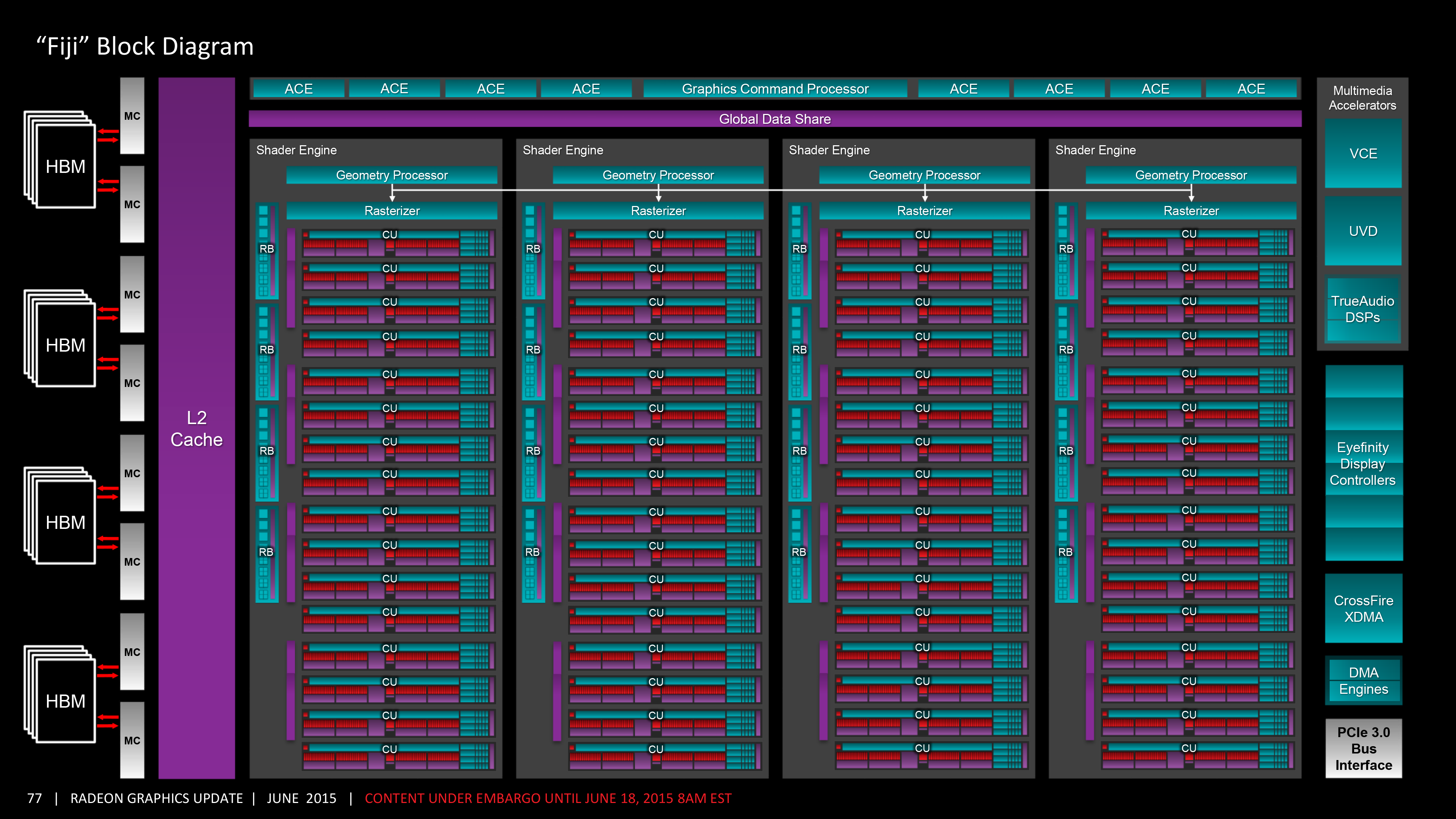
In either case the end result is quite a bit of shading power for Fiji. AMD has bumped up the CU count from 44 to 64, or to put this in terms of the number of ALUs/stream processors, it’s up from 2816 to a nice, round 4096 (2^12). As we discussed earlier FP64 performance has been significantly curtailed in the name of space efficiency, otherwise at Fury X’s stock clockspeed of 1050MHz, you’re looking at enough ALUs to push 8.6 TFLOPs of FP32 operations.
These 64 CUs in turn are laid out in a manner consistent with past GCN designs, with AMD retaining their overall Shader Engine organization. Sub-dividing the GPU into four parts, each shader engine possesses 1 geometry unit, 1 rasterizer unit, 4 render backends (for a total of 16 ROPs), and finally, one-quarter of the CUs, or 16 CUs per shader engine. The CUs in turn continue to be organized in groups of 4, with each group sharing a 16KB L1 scalar cache and 32KB L1 instruction cache. Meanwhile since Fiji’s CU count is once again a multiple of 16, this also does away with Hawaii’s oddball group of 3 CUs at the tail-end of each shader engine.
Looking at the broader picture, what AMD has done relative to Hawaii is to increase the number of CUs per shader engine, but not changing the number of shader engines themselves or the number of other resources available for each shader engine. At the time of the Hawaii launch AMD told us that the GCN 1.1 architecture had a maximum scalability of 4 shader engines, and Fiji’s implementation is consistent with that. While I don’t expect AMD will never go beyond 4 shader engines – there are always changes that can be made to increase scalability – given what we know of GCN 1.1’s limitations, it looks like AMD has not attempted to increase their limits with GCN 1.2. What this means is that Fiji is likely the largest possible implementation of GCN 1.2, with as many resources as the architecture can scale out to without more radical changes under the hood to support more scalability.
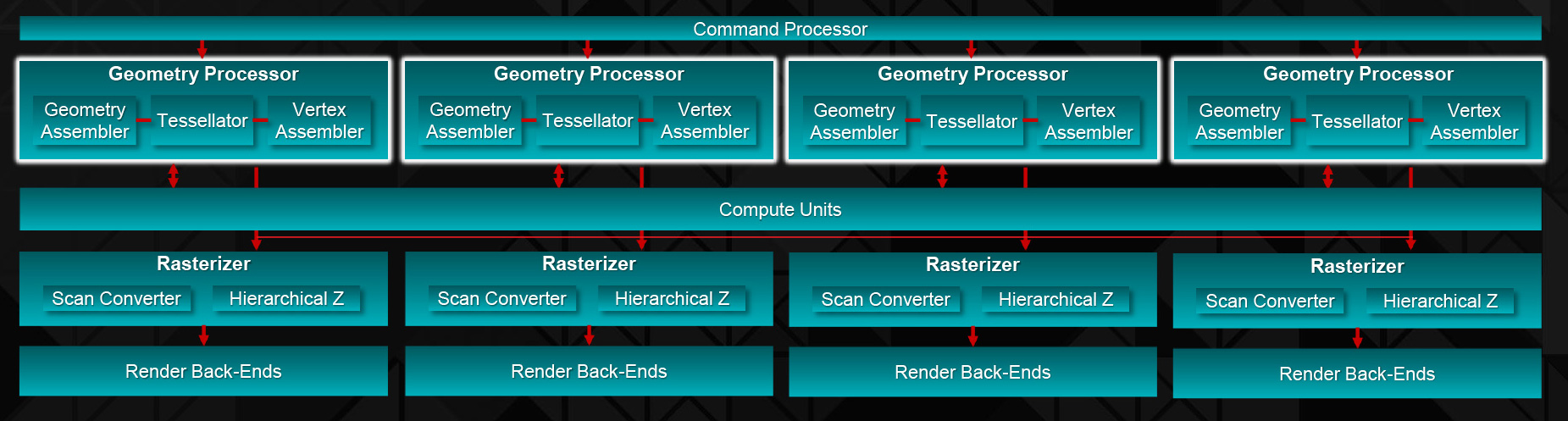
Along those lines, while shading performance is greatly increased over Hawaii, the rest of the front-end is very similar from a raw, theoretical point of view. The geometry processors, which as we mentioned before are organized to 1 per shader engine, just as was the case with Hawaii. With a 1 poly/clock limit here, Fiji has the same theoretical triangle throughput at Hawaii did, with real-world clockspeeds driving things up just a bit over the R9 290X. However as we discussed in our look at the GCN 1.2 architecture, AMD has made some significant under-the-hood changes to the geometry processor design for GCN 1.2/Fiji in order to boost their geometry efficiency, making Fiji’s geometry fornt-end faster and more efficient than Hawaii. As a result the theoretical performance may be unchanged, but in the real world Fiji is going to offer better geometry performance than Hawaii does.
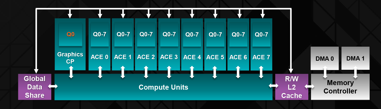
Meanwhile the command processor/ACE structure remains unchanged from Hawaii. We’re still looking at a single graphics command processor paired up with 8 Asynchronous Compute Engines here, and if AMD has made any changes to this beyond what is necessary to support the GCN 1.2 feature set (e.g. context switching, virtualization, and FP16), then they have not disclosed it. AMD is expecting asynchronous shading to be increasingly popular in the coming years, especially in the case of VR, so Fiji’s front-end is well-geared towards the future AMD is planning for.
Moving on, let’s switch gears and talk about the back-end of the processor. There are some significant changes here due to HBM, as to be expected, but there are also some other changes going on as well that are not related to HBM.
Starting with the ROPs, the ROP situation for Fiji remains more or less unchanged from Hawaii. Hawaii shipped with 64 ROPs grouped in to 16 Render Backends (RBs), which at the time AMD told us was the most a 4 shader engine GCN GPU could support. And I suspect that limit is still in play here, leading to Fiji continuing to pack 64 ROPs. Given that AMD just went from 32 to 64 a generation ago, another jump seemed unlikely anyhow (despite earlier rumors to the contrary), but in the end I suspect that AMD had to consider architectural limits just as much as they had to consider performance tradeoffs of more ROPs versus more shaders.
In any case, the real story here isn’t the number of ROPs, but their overall performance. Relative to Hawaii, Fiji’s ROP performance is getting turbocharged for two major reasons. The first is GCN 1.2’s delta color compression, which significantly reduces the amount of memory bandwidth the ROPs consume. Since the ROPs are always memory bandwidth bottlenecked – and this was even more true on Hawaii as the ROP/bandwidth ratio fell relative to Tahiti – anything that reduces memory bandwidth needs can boost performance. We’ve seen this first-hand on R9 285, which with its 256-bit memory bus had no problem keeping up with (and even squeaking past) the 384-bit bus of the R9 280.
The other factor turbocharging Fiji’s ROPs is of course the HBM. In case GCN 1.2’s bandwidth savings were not enough, Fiji also just flat-out has quite a bit more memory bandwidth to play with. The R9 290X and its 5Gbps, 512-bit memory bus offered 320GB/sec, a value that for a GDDR5-based system has only just been overshadowed by the R9 390X. But with Fiji, the HBM configuration as implemented on the R9 Fury X gives AMD 512GB/sec, an increase of 192GB/sec, or 60%.
Now AMD did not just add 60% more memory bandwidth because they felt like it, but because they’re putting that memory bandwidth to good use. The ROPs would still gladly consume it all, and this doesn’t include all of the memory bandwidth consumed by the shaders, the geometry engines, and the other components of the GPU. GPU performance has long outpaced memory bandwidth improvements, and while HBM doesn’t erase any kind of conceptual deficit, it certainly eats into it. With such a significant increase in memory bandwidth and combined with GCN 1.2’s color compression technology, AMD’s effective memory bandwidth to their ROPs has more than doubled from Hawaii to Fiji, which will go a long way towards increasing ROP efficiency and real-world performance. And even if a task doesn’t compress well (e.g. compute) then there’s still 60% more memory bandwidth to work with. Half of a terabyte-per-second of memory bandwidth is simply an incredible amount to have for such a large pool of VRAM, since prior to this only GPU caches operated that quickly.
Speaking of caches, Fiji’s L2 cache has been upgraded as well. With Hawaii AMD shipped a 1MB cache, and now with Fiji that cache has been upgraded again to 2MB. Even with the increase in memory bandwidth, going to VRAM is still a relatively expensive operation, so trying to stay on-cache is beneficial up to a point, which is why AMD spent the additional transistors here to double the L2 cache. Both AMD and NVIDIA have gone with relatively large L2 caches in this latest round, and with their latest generation color compression technologies it makes a lot of sense; since the L2 cache can store color-compressed tiles, all of a sudden L2 caches are a good deal more useful and worth the space they consume.
Finally, we’ll get to HBM in a more detail in a bit, but let’s take a quick look at the HBM controller layout. With Fiji there are 8 HBM memory controllers, and each HBM controller in turn drives one-half of an HBM stack, meaning 2 controllers are necessary to drive a full stack. And while AMD’s logical diagram doesn’t illustrate it, Fiji is almost certainly wired such that each HBM memory controller is tightly coupled with 8 ROPs and 256KB of L2 cache. AMD has not announced any future Fiji products with less than 4GB of VRAM, so we’re not expecting any parts with disabled ROPs, but if they did that would give you an idea of how things would be disabled.
Power Efficiency: Putting A Lid On Fiji
Last, but certainly not least, before ending our tour of the Fiji GPU we need to talk about power.
Power is, without question, AMD’s biggest deficit going into the launch of R9 Fury X. With Maxwell 2 NVIDIA took what they learned from Tegra and stepped up their power efficiency in a major way, which allowed them to not only outperform AMD’s Hawaii GPUs, but to do so while consuming significantly less power. In this 4th year of 28nm the typical power efficiency gains that come from a smaller process are another year off, so both AMD and NVIDIA have needed to invest in power efficiency at an architectural level for 28nm.
The power situation on Fiji in turn is a bit of a mixed bag, but largely positive for AMD. The good news here is that AMD has indeed taken power efficiency very seriously for Fiji, and in turn has made a number of changes to boost power efficiency and bring it more in line with what NVIDIA has achieved, leading to R9 Fury X being rated for the same 275W Typical Board Power (TBP) as the R9 390X, and just 25W more than R9 290X. The bad news, as we’ll see in our benchmarks, is that AMD won’t quite meet NVIDIA’s power efficiency numbers; but they had a significant gap to close and they have done a very admirable job in coming this far.
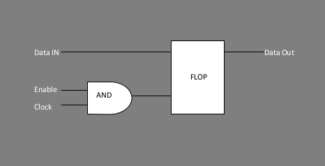
A basic implementation of clock gating. Image Source: Mahesh Dananjaya - Clock Gating
So what has AMD done to better control power consumption? Perhaps the biggest improvement here is that AMD has improved their clock gating technology by implementing multi-level clock gating throughout the chip, in order to better cut off parts of the GPU that are not in use and thereby reduce their power consumption. With clock gating the clock signal is turned off to a functional unit, leaving said unit turned on but not doing any work or switching transistors, which allows for significant power savings even without turning said unit off via power gating (and without the time-cost of bringing it back up). Even turning off a functional unit for a couple of dozen cycles, say while the geometry engines wait on the shaders to complete their work, brings down power consumption in load states as well as the more obvious idle states.
Meanwhile AMD has taken some lessons from their recently-launched Carrizo APU – which is also based on GCN 1.2 and designed around improving power efficiency – in order to boost power efficiency for Fiji. What AMD has disclosed to us is that the power flow for Fiji is based on what they’ve learned from the APUs, which in turn has allowed AMD to better control/map several aspects of Fiji’s voltage needs for better operation. Voltage adaptive operation, for example, allows AMD to use a lower voltage that’s closer to Fiji’s real voltage needs, reducing the amount of power wasted by operating Fiji at a voltage higher than it needs to operate. VAO essentially uses thinner voltage safeguards to accomplish this, pulling back the clockspeed momentarily if the supply voltage drops below Fiji’s operational requirements.
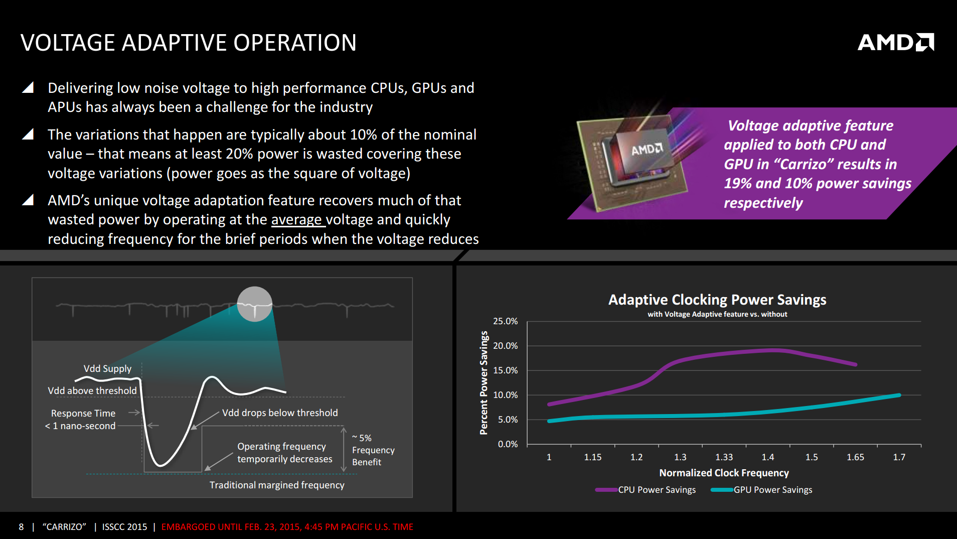
Similarly, AMD has also put a greater focus on the binning process to better profile chips before they leave the factory. This includes a tighter voltage/frequency curve (enabled by VSO) to cut down on wasted voltage, but it also includes new processes to better identify and compensate for leakage on a per-chip basis. Leakage is the eternal scourge for chip designers, and with 28nm it has only gotten worse. Even with the now highly-mature process, leakage can still consume (or rather allows to escape) quite a bit of power if not controlled for. This is also one of the reasons that FinFETs will be so important in TSMC’s next-generation 16nm manufacturing process, as FinFETs cut down on leakage.
AMD’s third power optimization comes from the use of HBM, which along with its greater bandwidth also offers lower power consumption relative to even the 512-bit wide 5Gbps GDDR5 memory bus AMD used on R9 290X. On R9 290X AMD estimates that memory power consumption was 15-20% (37-50W) of their 250W TDP, largely due to the extensive PHYs required to handle the complicated bus signaling of GDDR5.
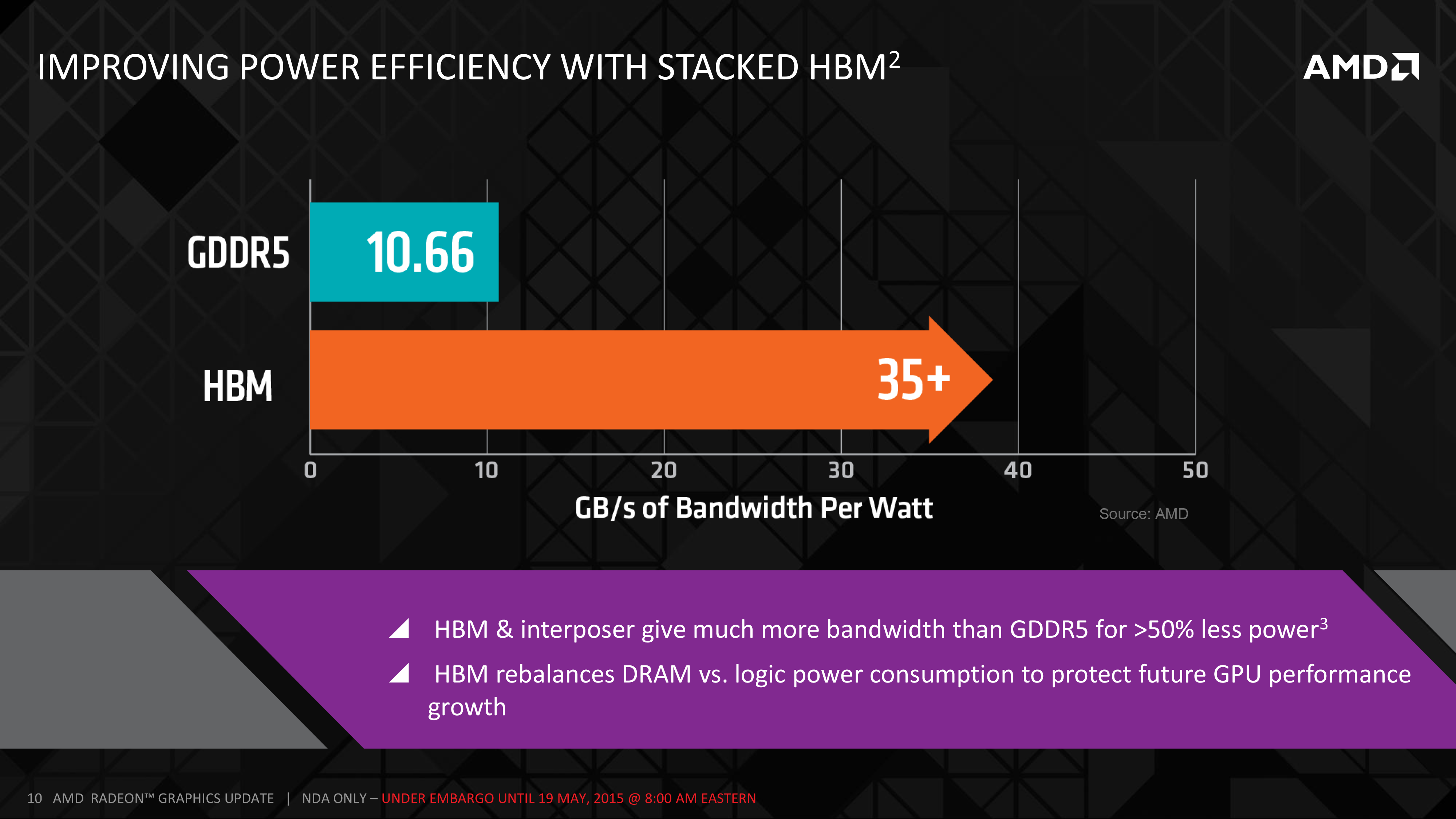
By AMD’s own metrics, HBM delivers better than 3x the bandwidth per watt of GDDR5 thanks to the simpler bus and lower operating voltage of 1.3v. Given that AMD opted to spend some of their gains on increasing memory bandwidth as opposed to just power savings, the final power savings aren’t 3X, but by AMD’s estimates the amount of power they’re spending on HBM is around 15-20W, which has saved R9 Fury X around 20-30W of power relative to R9 290X. These are savings that AMD can simply keep, or as in the case of R9 Fury X, spend some of them on giving the card more power headroom for higher performance.
The final element in AMD’s plan to improve energy efficiency on Fiji is a bit more brute-force but none the less important, and that’s temperature controls. As our long-time readers may recall from the R9 290 (Hawaii) launch in 2013, with the reference R9 290X AMD picked a higher temperature gradient over lower operating temperatures in order to maximize the cooling efficiency of their reference cooler. The tradeoff was that they had to accept higher leakage as a result of the higher temperatures, though as AMD’s second-generation 28nm product they felt they had leakage under control.
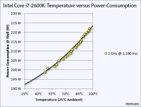
An example of the temperature versus power consumption principle on an Intel Core i7-2600K. Image Credit: AT Forums User "Idontcare"
But with R9 Fury X in particular and its large, overpowered closed loop liquid cooler, AMD has gone in the opposite direction. AMD no longer needs to rely on temperature gradients to boost cooler performance, and as a result they’ve significantly dialed down the average operating temperature of the Fiji GPU in R9 Fury X in order to further mitigate leakage and reduce overall power consumption. Whereas R9 290X would go to 95C, R9 Fury X essentially tops out at 65C, as that’s the point after which it will start ramping up the fan speed rather than allow the GPU to get any warmer. This 30C reduction in GPU temperature undoubtedly saves AMD some power on leakage, and while the precise amount isn’t disclosed, as leakage is a non-linear relationship the results could be rather significant for Fiji.
To put this to the test, we did a bit of experimenting with Crysis 3 to look at power consumption over time. While the R9 Fury X doesn’t allow us to let it run any warmer, we are able to monitor power consumption at the start of the benchmark run when the card has just left idle at around 40C, and compare it to when the run is terminated at 65C.
| Crysis 3 Power Consumption | ||||
| GPU Temperature | Power Consumption @ Wall | |||
| Start Of Run | 40C | 388W | ||
| 15 Minutes, Equilibrium | 65C | 408W | ||
What we find is that Fury’s power consumption increases by 20W at the wall between the start and the end, and this despite the fact that the scene is unchanged, the framerate is unchanged, and the CPU usage is unchanged. The roughly 18W difference after the PSU comes from the video card, its power consumption increasing with the GPU temperature and a slighter bump from the approximately 100RPM increase in fan speeds. Had AMD allowed Fury X to go to 83C (the same temperature as the GTX 980 Ti), it likely would have been closer to a 300W TBP card, and 95C would be higher yet, indicating just how important temperature controls are for AMD in order to get the best energy efficiency as is possible out of Fiji.
Last, but not least on the subject of power consumption, we need to quickly discuss the driver situation. AMD tells us that for R9 Fury X they were somewhat conservative on how they adjusted clockspeeds, favoring performance over power savings. As a result R9 Fury X doesn’t downclock as often as it could, staying at 1050MHz more often, practically running at maximum clockspeeds whenever a real load is put on it so that it offers the best performance possible should it be needed.
What AMD is telling us right now is that future drivers for Fiji products will be better tuned than what we’re seeing on Fury X, such that those parts won’t run at their full load clocks quite so aggressively. The nature of this claim invites a wait-and-see approach, but based on what we’re seeing with R9 Fury X so far, it’s not an unrealistic goal for AMD. More aggressive power control and throttling not only improves power consumption under light loads, but it also stands to improve power consumption under full load. GCN can switch voltages as quickly as 10 microseconds, or hundreds of times in the span of time it takes for a GPU to render a single frame, so there are opportunities there for the GPU to take short breaks whenever a bottleneck is occurring in the rendering process and the card’s full 1050MHz isn’t required for a thousand cycles or so.
On that note, AMD has also told us to keep our eyes peeled for what they deliver with the R9 Fury (vanilla). Without its closed loop liquid cooler, the R9 Fury will not have the same overbuilt cooling apparatus available, and as a result it sounds like AMD will take a more aggressive approach in-line with the above to better control power consumption.
High Bandwidth Memory: Wide & Slow Makes It Fast
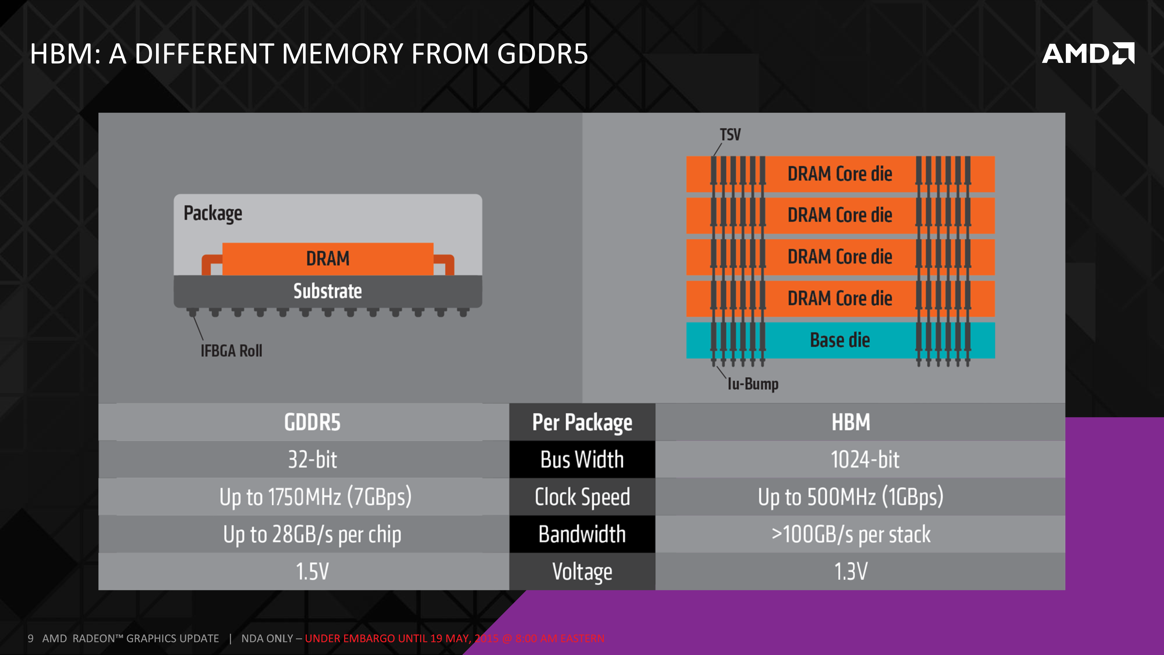
Architecturally, the single most notable addition to AMD’s collection of technologies for Fiji is High Bandwidth Memory (HBM). HBM is a next-generation memory standard that will ultimately come to many (if not all) GPUs as the successor to GDDR5. HBM promises a significant increase in memory bandwidth through the use of an ultra-wide, relatively low-clocked memory bus, with die stacked DRAM used to efficiently place the many DRAM dies needed to drive the wide bus.
As part of their pre-Fury X launch activities, AMD briefed the press on HBM back in May, offering virtually every detail one could want on HBM, how it worked, and the benefits of the technology. So for today’s launch there’s relatively little that’s new to say on the subject, but I wanted to quickly recap what we have seen so far.
After several years of GDDR5 – first used on the Radeon HD 4870 in 2008 – HBM comes at a time where GDDR5 is reaching its limits, and companies have been working on its successors. As awesome as GDDR5 is (and it delivers quite a bit of memory bandwidth compared to just about anything else), GDDR5 is already a bit of a power hog and rather complex to implement. GDDR5’s immediate successors would deliver more bandwidth, but they would also exacerbate this problem by drawing even more power and introducing all of the complexity inherent in differential I/O.
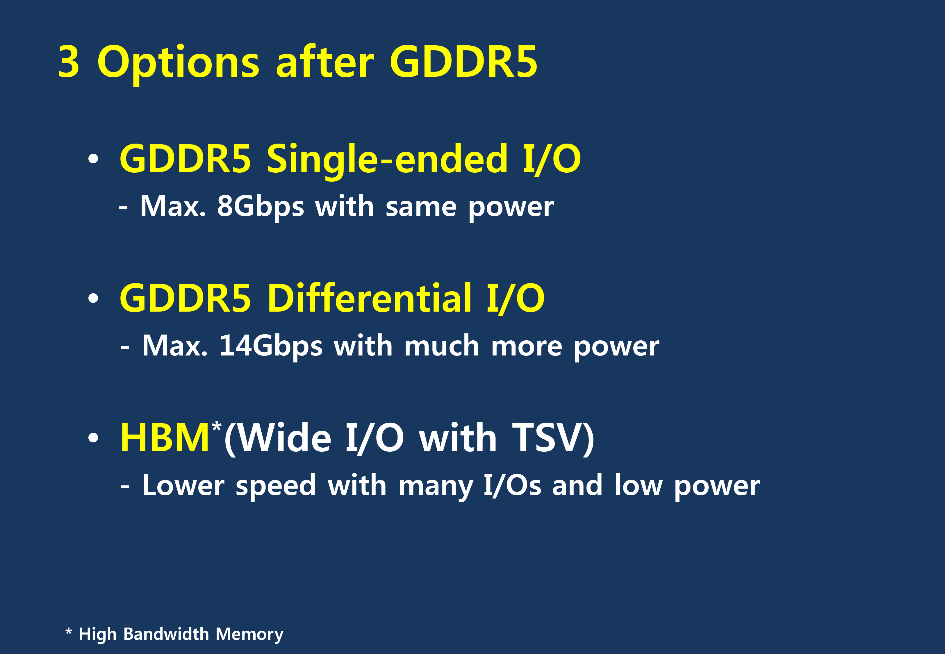
So to succeed GDDR5, AMD, Hynix, and the JEDEC as a whole have taken a very different path. Rather than attempting to push a very high bandwidth, narrow(ish) memory bus standard even higher, they have opted to go in the opposite direction with HBM. HBM would significantly back off of the clockspeeds used, but in return it would go wider than GDDR5. Much, much wider.
The ultimate direction that HBM takes us is with a very wide memory bus clocked at a low frequency. For Fiji, AMD has a 4096-bit memory bus clocked at 1000MHz (500MHz DDR). The use of such a wide bus more than offsets the reduction in clockspeed, allowing R9 Fury X to deliver 60% more memory bandwidth than the R9 290X’s GDDR5 implementation.
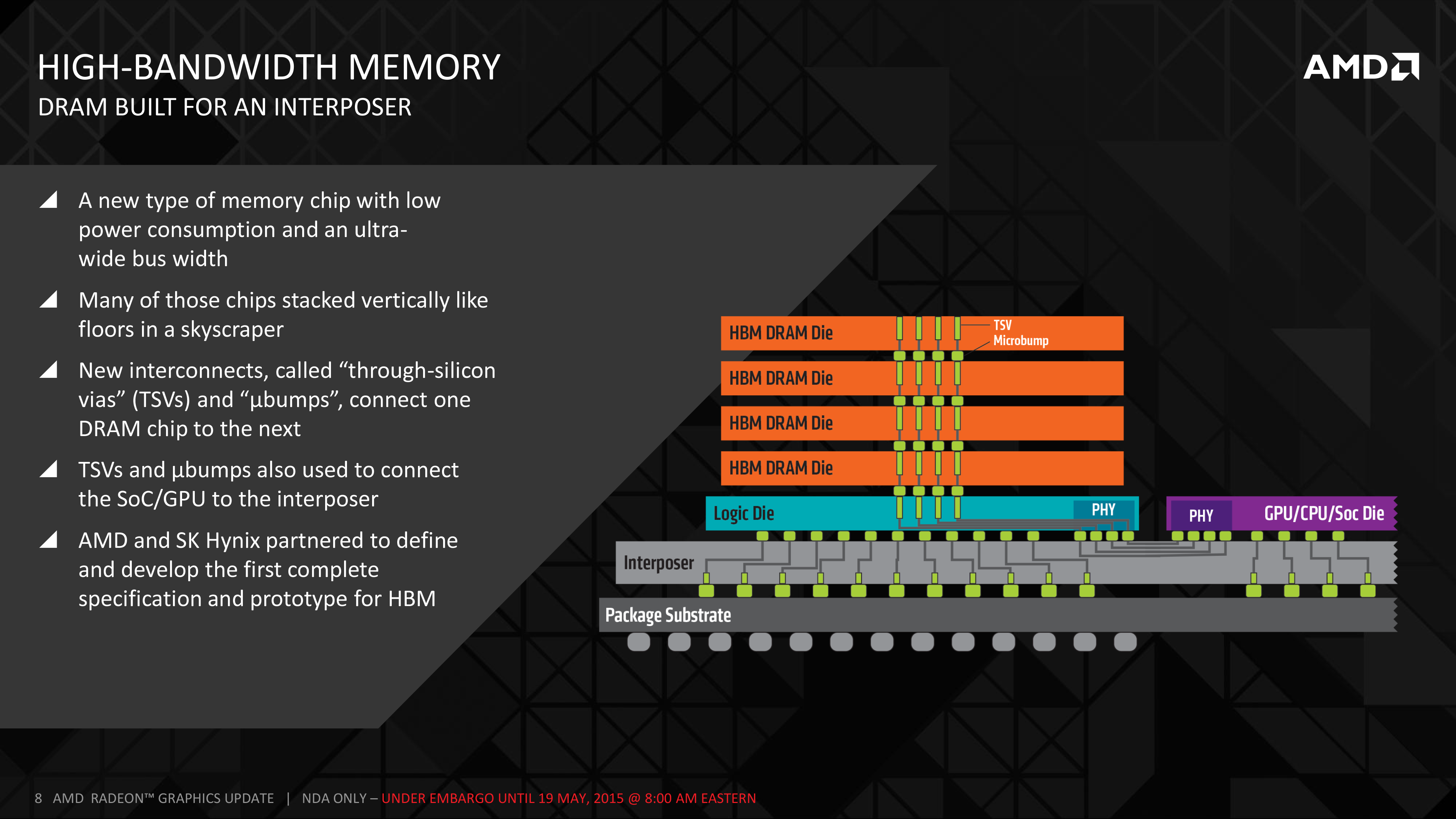
On the technical side of things, creating HBM has required a few different technologies to be created/improved in order to assemble the final product. The memory bus itself is rather simple (which is in and of itself a benefit), but a 4096-bit wide memory bus is by conventional standards absurdly wide. It requires thousands of contacts and traces, many times more than even 512-bit GDDR5 required (and that was already a lot).
To solve this problem HBM introduces the concept of a silicon interposer. With traditional packaging not up to the challenge of routing so many traces, the one material/package that is capable of hitting the necessary density is fabbed silicon, and thus the silicon interposer. Essentially a partially fabbed chip with just the metal layers but no logic, the interposer is a large chip whose purpose is to allow the ultra-wide 4096-bit memory bus to be created between a GPU and its VRAM, implemented as traces in the metal layers. The interposer itself is not especially complex, however because of the sheer size of the interposer (it needs to be large enough to hold the GPU and VRAM) the interposer brings with it its own challenges.
Meanwhile even though the interposer solves the immediate challenges of implementing a 4096-bit memory bus, the next issue that crops up is where to put the necessary DRAM dies. It takes 16 dies at 256-bits wide each to create the 4096-bit memory bus, and even at its largest size the interposer is still a fraction of the size of the PCB space that traditional GDDR5 chips occupy. As a result the DRAM required for an HBM solution needed to be denser than ever before in a 2D sense.
The solution to that problem was the creation of die-stacking the DRAM. If you can’t go wider, go taller, which is exactly what has happened with HBM. In HBM1 the stacks can go up to 4 dies high, allowing the necessary 16 dies to be reduced to a far more easily managed 4 stacks. With a base logic die at the bottom of each stack to serve as the PHY between the DRAM and the GPU (technically making the complete stack 5 dies), stacking the DRAM is what makes it practical to put so much RAM so close to the GPU.
The final new piece of technology in HBM comes in the die stacks themselves. With the need to route a 1024-bit memory bus through 4 memory dies, traditional package-on-package wire bonding is no longer sufficient. To connect up the memory dies, much like the interposer itself, a newer, denser connectivity method is required.

TSVs. Image Courtesy The International Center for Materials Nanoarchitectonics
To solve that problem, the HBM memory stacks implement Through-Silicon Vias, which involves running the vias straight through silicon devices in order to connect layers. The end result is something vaguely akin to DRAM dies surface mounted on top of each other via microbumps, but with the ability to communicate through the layers. From a manufacturing standpoint, between the silicon interposer and TSVs, TSVs are the more difficult technology to master as it essentially combines all the challenges of DRAM fabbing with the challenges of stacking those DRAM dies on top of each other.
Combined together as a single product, HBM is the next generation of GPU memory technology thanks to the fact that it offers multiple benefits over GDDR5. Memory bandwidth of course is a big part, but of similar significance is the power savings from HBM. The greatly simplified memory bus requires far less power be spent on the bus itself, and as a result the amount of power spent on VRAM is reduced. As we discussed earlier AMD is looking at a 20-30W VRAM power savings on R9 Fury X over R9 290X.
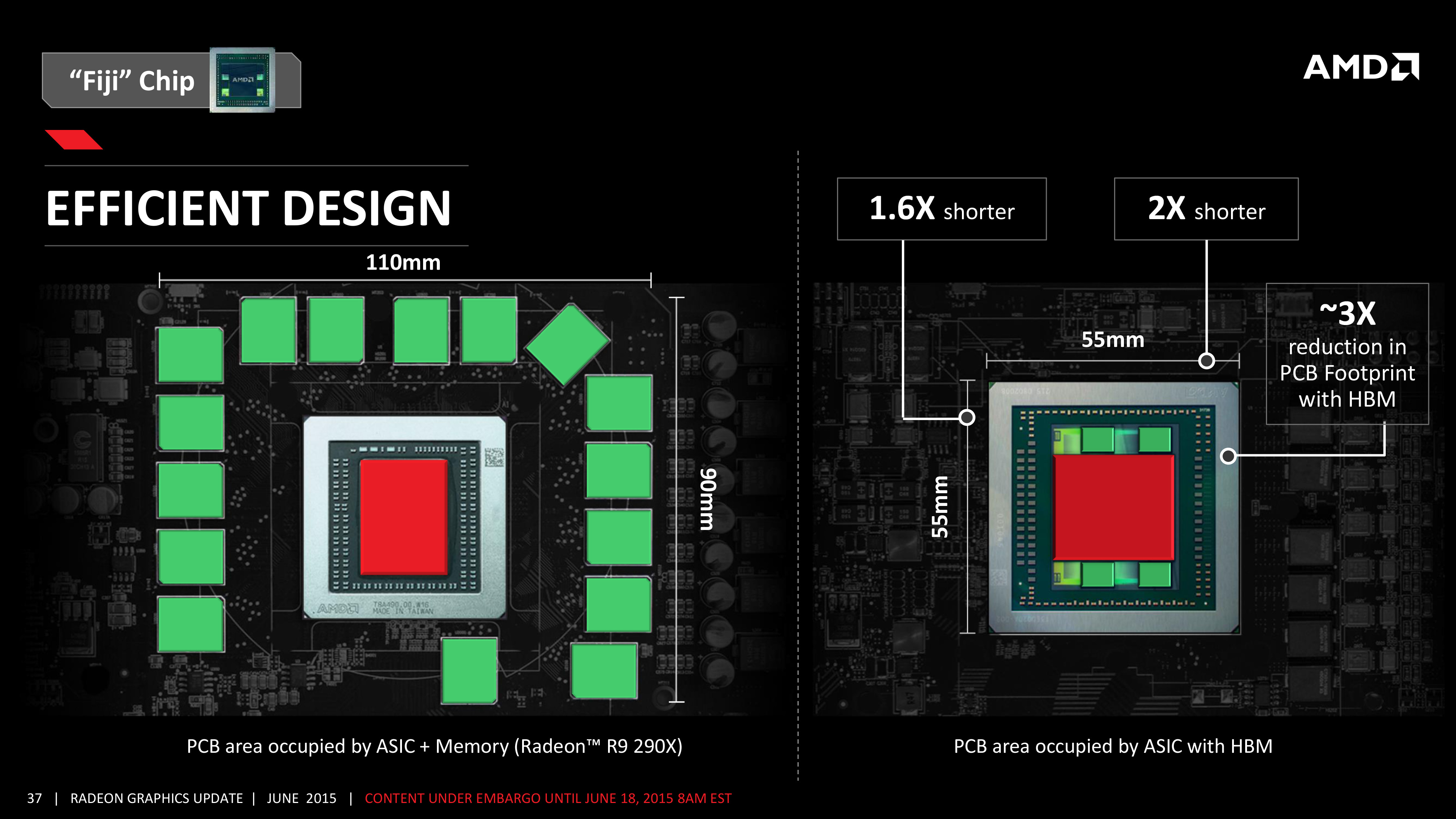
The third major benefit of HBM over GDDR5 goes back to the size benefits discussed earlier. Because all of the VRAM in an HBM setup fits on-chip, this frees up a significant amount of space. The R9 Fury X PCB is 3” shorter than the R9 290X PCB, and the bulk of these savings come from the space savings enjoyed by using HBM. Along with the immediate space savings of 4 small HBM stacks as opposed to 16 GDDR5 memory chips, AMD also gets to cut down on the amount of power delivery circuitry needed to support the VRAM, further saving space and some bill of material costs in the process.
On the downside though, it is the bill of materials that is the biggest question hanging over HBM. Since HBM introduces several new technologies there are any number of things that can go wrong, all of which can drive up the costs. Of particular concern is the yield on the HBM memory stacks, as the TSV technology is especially intricate and said to be difficult to master. The interposer on the other hand is simpler, but it still represents something that has never been done before, and AMD admits upfront that the manufacturing facilities being used to create the interposer are old 65nm lines originally used for full chip production. So while the interposer does not approach the cost of a full logic chip, there is still the matter of the existing manufacturing lines being sub-optimal for high-volume low-cost production. Meanwhile AMD does get to enjoy some cost savings as well – the HBM PHYs are certainly much easier to implement than GDDR5 PHYs on Fiji itself, and the overall package is cheaper since it doesn't have GDDR5 memory running through it – though it's unlikely that these savings outweigh the other costs of implementing HBM at this time.
Ultimately AMD Is not willing to discuss HBM costs or yields at this time. Practically speaking it’s not a consumer matter – what matters to video card buyers is the $650 price tag on the R9 Fury X – and from a trade secrets perspective AMD is loath to share too much about what they have learned since they are the first HBM customer and want to enjoy as much of that advantage as is possible. At this point I feel it’s a safe bet that the 4GB HBM implementation on Fiji is costing AMD more than the 4GB (or even 8GB) GDDR5 implementations on Hawaii cards, but beyond that it’s difficult to say much more on costs.
That said, regardless of what the costs are now, HBM will be the future for AMD, and for the GPU industry as a whole. NVIDIA has already committed to using HBM technology for their high-end Pascal GPU in 2016, so AMD will be joined by other parties next year. Meanwhile AMD has much grander plans for HBM, intending to bring it to other products as costs allow. HBM on lower-priced GPUs is practically a given, meanwhile equipping AMD’s APUs with HBM would solve one of the greatest problems AMD faces today on the iGPU performance front, which is that 128-bit DDR3 bottlenecks the iGPU on their Kaveri APUs. AMD could build a better iGPU, if only they had more bandwidth to feed it with. This is a problem HBM is well positioned to solve.
Finally, at the end of the day what can’t be perfectly captured in words is AMD’s pride in being the first to roll out HBM. AMD was the first (and only) company to support GDDR4, they were the first company to support GDDR5, and now they are the first company to support HBM. The company has put significant resources into helping to develop the technology alongside Hynix, UMC, ASE, Amkor, and the JEDEC, and they see the launch of the technology as a testament to their engineering capabilities.
Furthermore they also see the fact that they are first as being a significant advantage going forward, as it means they have a generational advantage on arch-rival NVIDIA in implementing the technology. Case in point, NVIDIA’s first GDDR5 memory controller was by all accounts an underperformer, and it wasn’t until their second generation GDDR5 controller for Kepler that NVIDIA was able to hit (and even exceed) their aimed for memory clockspeeds. Admittedly this comes down to AMD hoping NVIDIA is going to stumble here, but at the end of the day the company is optimistic that all of their work is going to allow them to get more out of HBM than NVIDIA will be able to.
HBM: The 4GB Question
Having taken a look at HBM from a technical perspective, there’s one final matter to address with Fiji’s implementation of HBM, and that is the matter of capacity.
For HBM1, the maximum capacity of a HBM stack is 1GB, which in turn is made possible through the use of 4 256MB (2Gb) memory dies. With a 1GB/stack limit, this means that AMD can only equip the R9 Fury X and its siblings with 4GB of VRAM when using 4 stacks. Larger stacks are not possible, and while in principle it would be possible to do an 8 stack HBM1 design, doing so would double the width of the memory bus and invite a whole slew of issues with it at the same time. Ultimately for reasons ranging from interposers to where to place the stacks, the most AMD can get out of HBM1 is 4GB of VRAM.
To address the elephant in the room then, the question arises of whether 4GB is going to be enough VRAM. 4GB is as much VRAM as was on the R9 290X in 2013, it’s as much VRAM as was on the GTX 980 in 2014. But it’s also less VRAM than the 6GB that is on the GTX 980 Ti in 2015 (never mind the GTX Titan X at this point) and it’s less VRAM than the 8GB that is on the just-launched R9 390X. Even ignoring NVIDIA for a moment, R9 Fury X offers less VRAM than AMD’s next-lower tier of video cards.
This is quite a bit of a role reversal in the video card industry, as traditionally AMD has offered more VRAM than the competition. Thanks in large part to their favoring wider memory buses (which means more memory chips), AMD has offered greater memory capacities at similar prices than traditionally stingy NVIDIA. Now however they are on the other foot, and the timing is not all that great.
| Console Memory Capacity | |||
| Capacity | |||
| Xbox 360 | 512MB (Shared) | ||
| Playstation 3 | 256MB + 256MB | ||
| Xbox One | 8GB (Shared) | ||
| Playstation 4 | 8GB (Shared) | ||
| Fiji | 4GB (Dedicated VRAM) | ||
Perhaps the single biggest influence here over VRAM requirements right now is the current-generation consoles, which launched back in 2013 with 8GB of RAM each. To be fair to AMD and to be technically correct these are shared memory devices, so that 8GB gets split between GPU resources and CPU resources, and even this comes after Microsoft and Sony set aside a significant amount of memory for their OSes and background tasks. Still, when using the current-gen consoles as a baseline, the current situation makes it possible to build a game that requires over 4GB of VRAM (if only just over), and if that game is naïvely ported over to the PC, there could be issues.
Throwing an extra wrench into things is that PCs have more going on than just console games. PC gamers buying high-end cards like the R9 Fury X will be running at resolutions greater than 1080p and likely with higher quality settings than the console equivalent, driving up the VRAM requirements. The Windows Desktop Window Manager responsible for rendering and compositing the different windows together in 3D space consumes its own VRAM as well. So the current PC situation pushes VRAM requirements higher still.
The reality of the situation is that AMD knows where they stand. 4GB is the most they can equip Fiji with, so it’s what they will have to make-do with until HBM2 comes along with greater densities. In the meantime the marketing side of AMD needs to convince potential buyers that 4GB is enough, and the technical side of AMD needs to come up with other solutions to help mitigate the problem.
On the latter point, while AMD can’t do anything about the amount of VRAM they have, they can and are working on doing a better job of using it. AMD has been rather straightforward in admitting that up until now they’ve never seriously dedicated resources to VRAM management on their cards, as they’ve always had enough VRAM that they have never considered it an issue. Until Fiji there was always enough VRAM.
Which is why for Fiji, AMD tells us they have dedicated two engineers to the task of VRAM optimizations. To be clear here, there’s little AMD can to do reduce VRAM consumption, but what they can do is better manage what resources are placed in VRAM and what resources are paged out to system RAM. Even this optimization can’t completely resolve the 4GB issue, but it can help up to a point. So long as game isn’t actively trying to use all 4GB of resources at once, then intelligent paging can help ensure that only the resources that are actively in use reside in VRAM and therefore are immediately available to the GPU when requested.
As for the overall utility of this kind of optimization, it’s going to depend on a number of factors, including the OS, the game’s own resource management, and ultimately the real working set needs of a game. The situation AMD faces right now is one where they have to simultaneously fight an OS/driver paradigm that wastes memory, and the games that will be running on their GPUs traditionally treat VRAM like it’s going out of style. The limitations of DirectX 11/WDDM 1.x prevent full reuse of certain types of assets by developers, and all the while it’s extremely common for games to claim much (if not all) available VRAM for their own use with the intent of ensuring they have enough VRAM for future use, and otherwise caching as many resources as possible for better performance.
The good news here is that the current situation leaves overhead that AMD can optimize around. AMD has been creating both generic and game-specific memory optimizations in order to better manage VRAM usage and what resources are held in local VRAM versus paging out to system memory. By controlling duplicate resources and clamping down on overzealous caching by games, it is possible to get more mileage out of the 4GB of VRAM AMD has.
Longer term, AMD is looking at the launch of Windows 10 and DirectX 12 to change the situation for the better. The low-level API will allow careful developers to avoid duplicate assets in the first place, and WDDM 2.0 overall is said to be a bit nicer about how it handles VRAM consumption. None the less the first DirectX 12 games aren’t launching for a few more months, and it will be longer still until those games are in the majority. As a result the situation AMD faces is one where they need to do well with Windows 8.1 and DirectX 11 games, as those games aren’t going anywhere right away and they will be the games that stress Fiji the most.
So with that in mind, let’s attempt to answer the question at hand: is 4GB enough VRAM for R9 Fury X? Is it enough for a $650 card?
The short answer is yes, at the moment it’s enough, if just barely.
To be clear, we can without fail “break” the R9 Fury X and place it in situations where performance nosedives because it has run out of VRAM. However of the tests we’ve put together, those cases are essentially edge cases; any scenario we come up with that breaks the R9 Fury X also results in average framerates that are too low to be playable in the first place. So it is very difficult (though I do not believe impossible) to come up with a scenario where the R9 Fury X would produce playable framerates if only it had more VRAM.
Case in point, in our current gaming test suite Shadows of Mordor and Grand Theft Auto V are the two most VRAM-hungry games. Attempting to break the R9 Fury X with Shadow of Mordor is ineffective at best; even with the HD texture pack installed (which is not the default for our test suite) the game’s built-in benchmark hardly registers a difference. Both the average and minimum framerates are virtually unchanged from our results without the HD texture pack. Meanwhile playing the game is much the same, though it’s entirely possible there are scenarios in the game not covered by that or the benchmark where more than 4GB of VRAM is truly required.
| Breaking Fiji: VRAM Usage Testing | ||||
| R9 Fury X | GTX 980 Ti | |||
| Shadows of Mordor Ultra, Avg | 47.7 fps | 49 fps | ||
| Shadows of Mordor Ultra, Min | 31.6 fps | 38 fps | ||
| GTA V, "Breaker", Avg | 21.7 fps | 26.2 fps | ||
| GTA V, "Breaker", 99th Perc. | 6 fps | 17.8 fps | ||
Meanwhile with GTA5 we can break the R9 Fury X, but only at unplayable settings. The card already teeters on the brink with our standard 4K “Very High” settings, which includes 4x MSAA but no “advanced” draw distance enhancements, with minimum framerates well below the GTX 980 Ti. Turning up the draw distance in turn further halves those minimums, driving the minimum framerate to 6fps as the R9 Fury X is forced to swap between VRAM and system RAM over the very slow PCIe bus.
But in both of these cases the average framerate is below 30fps (never mind 60fps), and not just for the R9 Fury X, but for the GTX 980 Ti as well. No scenario we’ve tried that breaks the R9 Fury X leaves it or the GTX 980 Ti running a game at 30fps or better, typically because in order to break the R9 Fury X we have to run with MSAA, which is itself a performance killer.
Unfortunately for AMD they are pushing the R9 Fury X as a 4K gaming card, and for a good reason. AMD’s performance traditionally scales better with resolution (i.e. deteriorates more slowly), so AMD’s best chance of catching up to NVIDIA is at 4K. However this also stresses R9 Fury X’s 4GB of VRAM all the more, which puts them in VRAM-limited situations all the sooner. It’s not quite a catch-22 situation, but it’s also not a situation AMD is going to want to be in.
Ultimately even at 4K AMD is okay for the moment, but only just. If VRAM requirements increase any more than they already have – if games start requiring 6-8GB at the very high end – then the R9 Fury X (and every other 4GB card for that matter) is going to be in trouble. And in the meantime anything worse than 4K, be it multi-monitor setups or 5K displays, is going to exacerbate the problem.
AMD believes their situation will get better with Windows 10 and DirectX 12, but until DX12 games actually come out in large numbers, all we can do is look at the kind of games we have today. And right now what we’re seeing are signs that the 4GB era is soon to come to an end. 4GB is enough right now, but I suspect 4GB cards now have less than 2 years to go until they’re undersized, which is a difficult situation to be in for a $650 video card.
Display Matters: Virtual Super Resolution, Frame Rate Targeting, and HEVC Decoding
Wrapping up our look at the technical underpinnings of the Fiji GPU, we’ll end things with a look at the display and I/O stack for AMD’s latest GPU.
As a GCN 1.2 part, Fiji inherits most of its capabilities in-place from Tonga. There is one notable exception to this, HEVC, which we’ll get to in a bit, otherwise from a features standpoint you’re looking at the same display feature set as was on Tonga.

For Display I/O this means 6 display controllers capable of driving DVI, HDMI 1.4a, and DisplayPort 1.2a. Unfortunately because Tonga lacked support for HDMI 2.0, the same is true for Fiji, and as a result you can only drive 4k@60Hz displays either via DisplayPort, or via tandem HDMI connections. The good news here is that it will be possible to do active conversion from DisplayPort to HDMI 2.0 later this year, so Fiji is not permanently cut-off from HDMI 2.0, however those adapters aren’t here quite yet and there are still some unresolved questions to be addressed (e.g. HDCP 2.2).
On the multimedia front, Fiji brings with it an enhanced set of features from Tonga. While the video encode side (VCE) has not changed – AMD still supports a wide range of H.264 encode settings – the video decode side has seen a significant upgrade. Fiji is the first AMD discrete GPU to support full hardware HEVC decoding, coinciding with the launch of that feature on the GCN 1.2-based Carrizo APU as well.
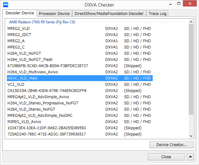
A look at DXVA Checker confirms the presence of Main Profile (HEVC_VLD_Main) support, the official designation for 8-bit color support. Main profile is expected to be the most common profile level for HEVC content, so Fiji’s support of just Main profile should cover many use cases.
Unfortunately what you won’t find here is Main10 profile support, which is the profile for 10-bit color, and AMD has confirmed that 10-bit color support is not available on Fiji. As our in-house video guru Ganesh T S pointed out when looking at these results, Main10 is already being used in places you wouldn’t normally expect to see it, such as Netflix streaming. So there is some question over how useful Fiji’s HEVC decoder will be with commercial content, ignoring for now the fact that lack of Main10 support essentially rules out good support for some advanced color space features such as Rec. 2020, which needs higher bit depths to support the larger color space without extensive banding.
Meanwhile the state of AMD’s drivers with respect to video playback is hit and miss. DXVA Checker crashed when attempting to enumerate 4K resolution support on Fiji, and 4K has been something of a thorn in AMD’s side. This is also likely why Media Player Classic Home Cinema and its built-in LAV Filters are currently ignoring 4K support on Fiji and are falling back to software decoding. As a result 1080p hardware decoding works great on Fiji – both H.264 and HEVC – but getting Fiji to decode 4K content is a lot harder. Using Windows’ built-in H.264 decoder works for 4K H.264 decoding, and in the meantime it’s a bit harder to test Fiji’s HEVC capabilities at 4K since Windows 8 lacks an HEVC decoder.
Decoding 1080p HEVC In MPC-HC on Fiji
With full hardware decode support for HEVC still being relatively new in the PC space, I expect we’ll see some teething issues for some time yet. For the moment AMD needs to resolve any crashing issues and get off of LAV’s blacklist, since the LAV filters are by our estimation the most commonly used for generic HEVC media playback.
On a side note, given the fact that the Tonga GPU (R9 285) is the only GCN 1.2 GPU without HEVC decoding, I also took the liberty of quickly loading up a modified copy of the Catalyst 15.15 launch drivers for the R9 300/Fury series, and seeing if HEVC support may have been hidden in there the entire time. Even with these latest drivers, R9 285 does not support HEVC, and while I admittedly wasn’t expecting it to, I suspect there’s more to Tonga’s UVD block given its nature as the odd man out.
Last but not least, TrueAudio support is also included with Fiji. First introduced on AMD’s GCN 1.1 family, TrueAudio is AMD’s implementation of advanced hardware audio processing, powered by a cluster of Tensilica’s HiFi EP DSPs. Despite these DSPs being similar to what’s found on the PS4, we have not seen much in the way of support for TrueAudio in the last year outside of a few AMD-sponsored demos/titles, so thus far it remains an underutilized hardware feature.
Moving on, let’s talk software features. Back in December with their Omega Drivers, AMD introduced Virtual Super Resolution. VSR is AMD’s implementation of downsampling and is essentially the company’s answer to NVIDIA’s DSR technology.
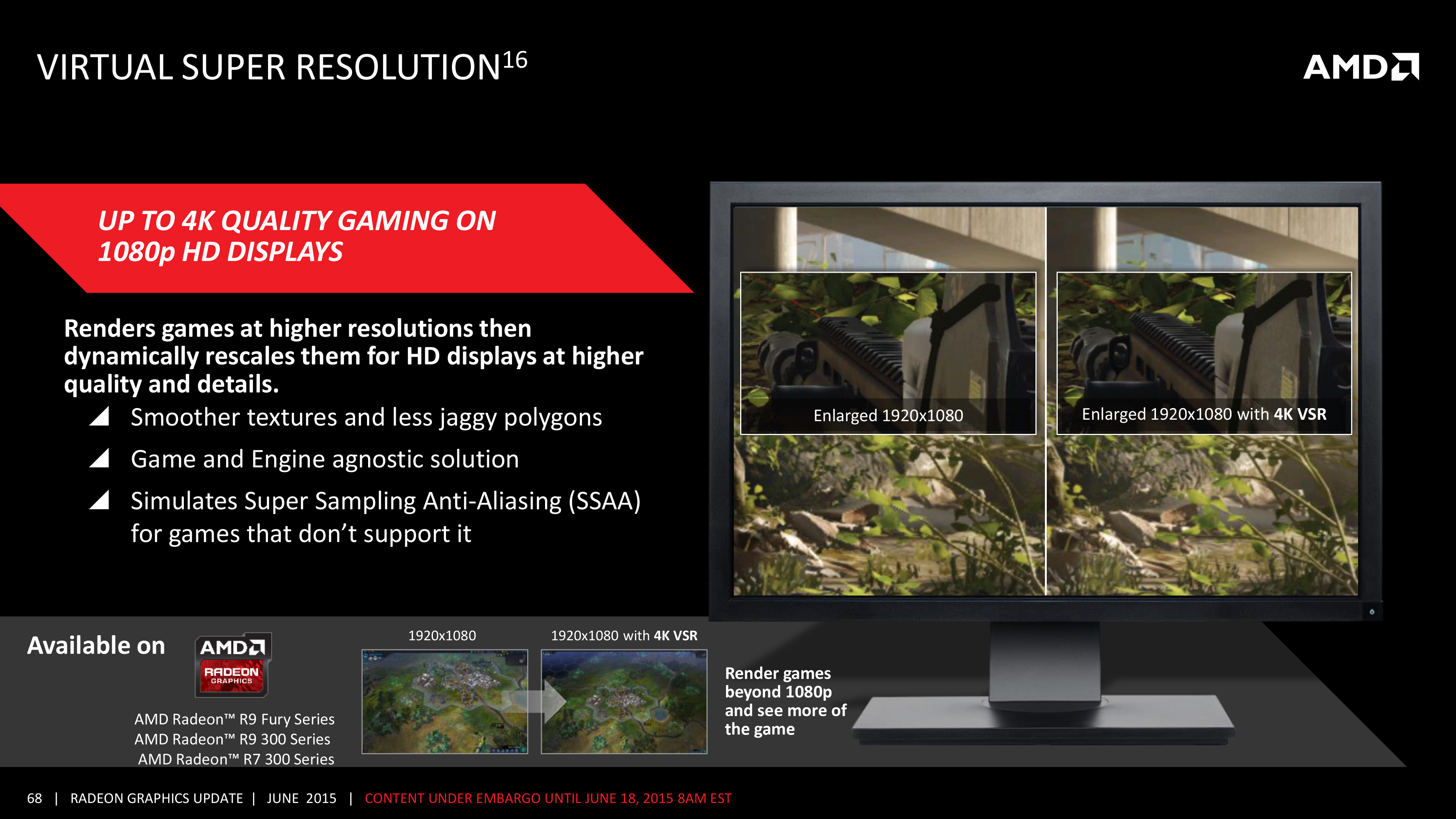
However while VSR and DSR are designed to solve the same problem, the two technologies go about solving it in very different ways. With DSR NVIDIA implemented it as a shader program; it gave NVIDIA a lot of resolution flexibility in exchange for a slight performance hit, and for better or worse they threw in a Gaussian blur by default as well. AMD however opted to implement VSR directly against their display controllers, skipping the shading pipeline and the performance hit at a cost of flexibility.
Due to the nature of VSR and the fact that it heavily relies on the capabilities of AMD’s display controllers, only AMD’s newest generation display controllers offer the full range of virtual resolutions. The GCN 1.1 display controller, for example, could not offer 4K virtual resolutions, so the R9 290X and other high-end Hawaii cards topped out at a virtual resolution of 3200x1800 for 1080p and 1440p displays. With GCN 1.2 however, AMD’s newer display controller supports downsampling from 4K in at least some limited scenarios, and while this wasn’t especially useful for the R9 285, this is very useful for the R9 Fury X.
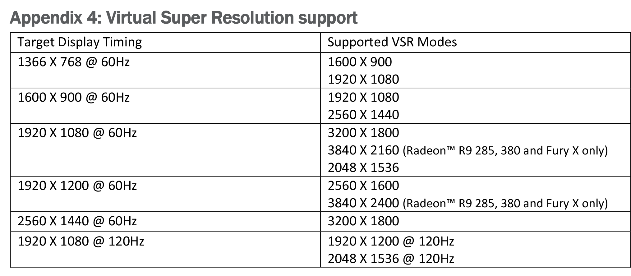
Overall for the R9 Fury X, the notable downsampling modes supported for the card are 3200x1800 (2.77x) and 3840x2160 (4.0x) for a native resolution of 1080p, 2560x1600 (1.77x) and 3840x2400 (4.0x) for a native resolution of 1200p, and unfortunately just 3200x1800 (1.56x) for a native resolution of 1440p. As a result VSR still can’t match the flexibility of DSR when it comes to resolutions, but AMD can finally offer 4K downsampling for 1080p panels, which allows for a nice (but expensive) 2x2 oversampling pattern, very similar to 4x ordered grid SSAA.
Finally, with AMD’s latest drivers they are also introducing a new framerate capping feature they are calling Frame Rate Target Control (FRTC). FRTC itself is not a new concept – 3rd party utilities such as MSI Afterburner and Radeon Pro have supported such functionality for a number of years now – however the change here is that AMD is finally bringing the technology into their drivers rather than requiring users to seek out 3rd party tools to do the job.
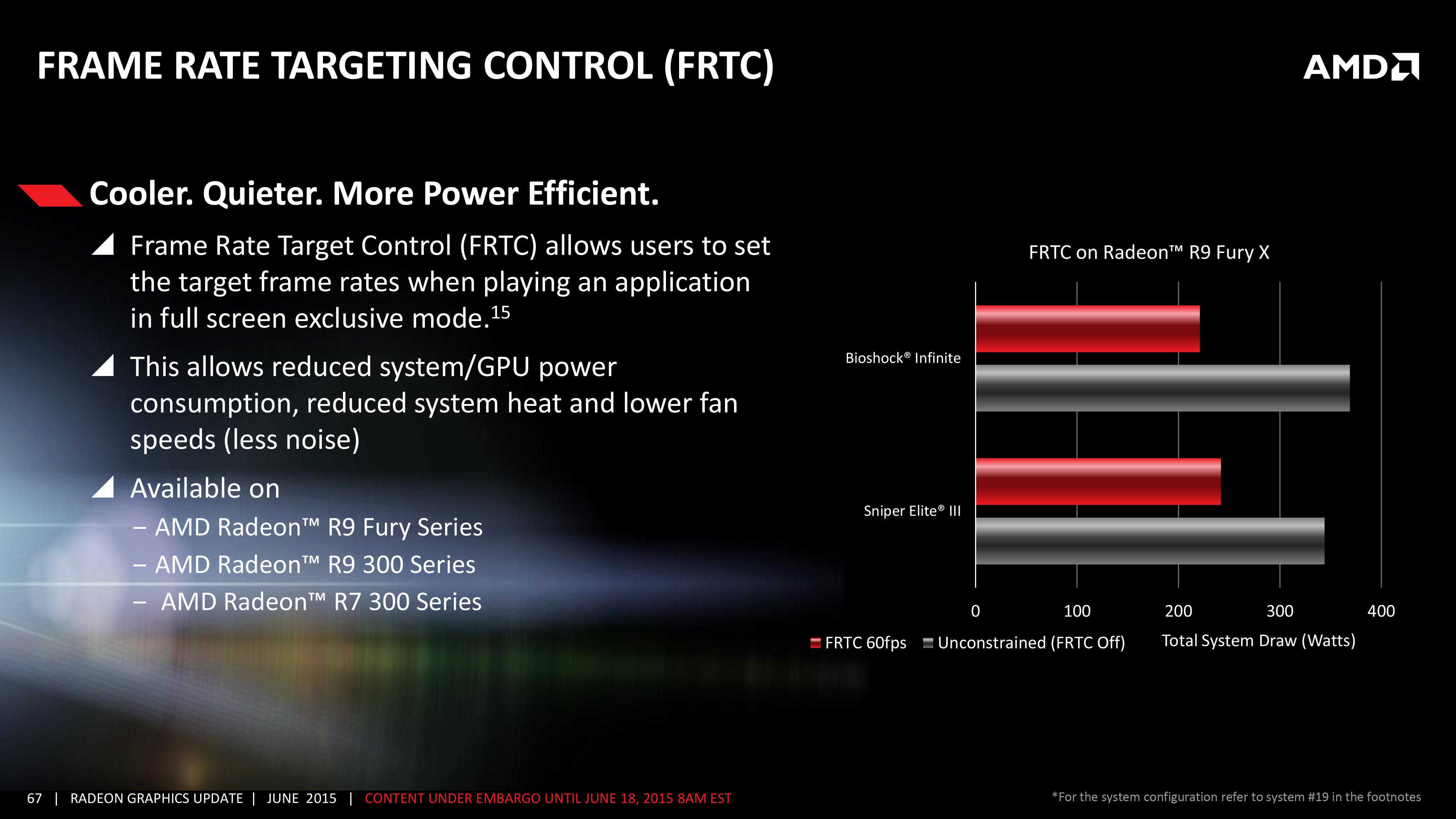
Frame Rate Target Control: From 55 fps to 95 fps
The purpose of FRTC is to allow users to cap the maximum framerate of a game without having to enable v-sync and the additional latency that can come from it, making for an effective solution that not v-sync and yet still places a hard cap on framerates. Note however that this is not a dynamic technology (ala NVIDIA’s Adaptive Sync), so there is no ability to dynamically turn v-sync on and off here. As for why users might want to cap their framerates, this is primarily due to the fact that video cards like the R9 Fury X can run circles around most older games, rendering framerates in to the hundreds at a time when even the fastest displays top out at 144Hz. Capping the frame rate serves to cut down on unnecessary work as a result, keeping the GPU from rendering frames that will never be seen.
AMD is only advertising FRTC support for the 300/Fury series at this time, so there is some question over whether we will see it brought over to AMD’s older cards. Given that AMD’s drivers are essentially split at the moment, I suspect we won’t have our final answer until the drivers get re-unified in a later release (most likely this month).
The Four Faces of Fiji, & Quantum Too
All told, AMD has announced that they will be launching 4 different video cards based on the Fiji GPU in the coming months. Today’s launch is for their single-GPU flagship, the R9 Fury X, but that card will soon be joined by single-GPU and multi-GPU siblings.
| AMD Planned Fiji Cards | ||||||
| AMD Radeon R9 Fury X | AMD Radeon R9 Fury | AMD Radeon R9 Nano | AMD Dual Fiji Card | |||
| Stream Processors | 4096 | (Fewer) | 4096 | 2 x ? | ||
| Texture Units | 256 | (How much) | 256 | 2 x ? | ||
| ROPs | 64 | (Depnds) | 64 | 2 x 64 | ||
| Boost Clock | 1050MHz | (On Yields) | (Lower) | ? | ||
| Memory Clock | 1Gbps HBM | (Memory Too) | (Unknown) | ? | ||
| Memory Bus Width | 4096-bit | 4096-bit | 4096-bit | 2 x 4096-bit | ||
| VRAM | 4GB | 4GB | 4GB | 2 x 4GB | ||
| FP64 | 1/16 | 1/16 | 1/16 | 1/16 | ||
| TrueAudio | Y | Y | Y | Y | ||
| Transistor Count | 8.9B | 8.9B | 8.9B | 2 x 8.9B | ||
| Typical Board Power | 275W | (High) | 175W | ? | ||
| Manufacturing Process | TSMC 28nm | TSMC 28nm | TSMC 28nm | TSMC 28nm | ||
| Architecture | GCN 1.2 | GCN 1.2 | GCN 1.2 | GCN 1.2 | ||
| GPU | Fiji | Fiji | Fiji | Fiji | ||
| Launch Date | 06/24/15 | 07/14/15 | "Summer" | "Fall" | ||
| Launch Price | $649 | $549 | (Unknown) | (Unknown) | ||
The second Fiji card to be launched will be the R9 Fury (vanilla) later this month. AMD has not announced the specifications for this card – presumably to avoid taking any attention away from the R9 Fury X and from any risk of Osborning it in the process – but we do know a few things about the card. Unlike the R9 Fury X, the R9 Fury will be an air cooled card, with AMD’s partners putting together their own designs for the card. It will be based on a cut down version of the Fiji GPU – so you won’t be seeing any air cooled full-performance Fiji cards – though it, like all Fiji cards, will come with all 4GB of VRAM. Finally, it will be launching at $549.
For AMD’s third Fiji card, they are going small form factor, and this is the card that will be called the R9 Nano (the lack of Fury in the name is intentional). Taking advantage of the highly integrated nature of the Fiji GPU and the resulting small boards that can be built with it, AMD will be producing a card similar in size to the R9 Fury X, except with air cooling rather than liquid cooling. The R9 Nano turned a lot of heads when it was first introduced and for good reason; while cards optimized for small form factors are not a new thing, they tend to top out at mid-to-high end GPUs, such as Tonga and GM204. The R9 Nano would be substantially more powerful by comparison, but no larger.
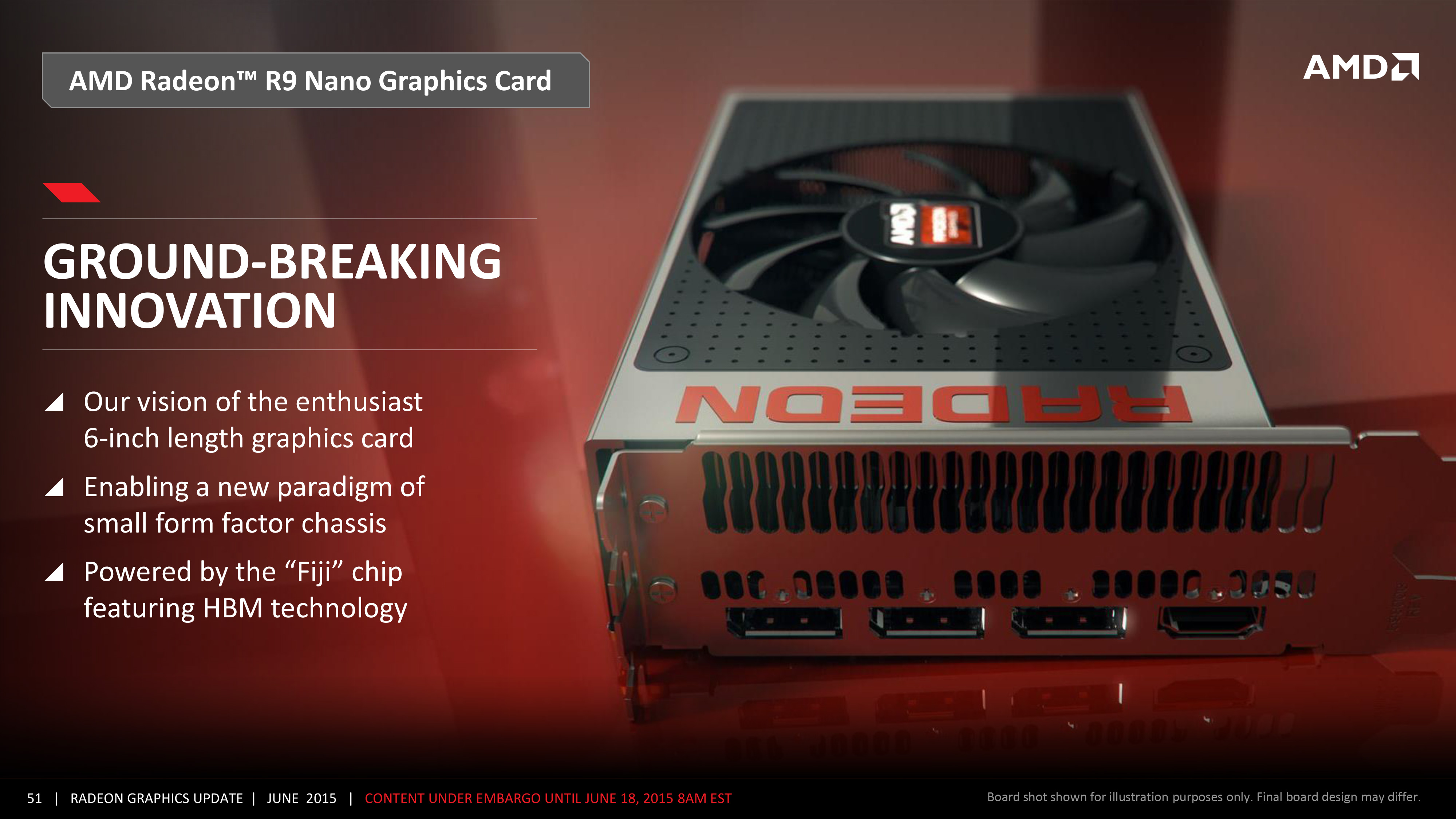
Unlike the R9 Fury, AMD has announced the bulk of the specs for the R9 Nano. This card will feature a fully enabled Fiji GPU, and given AMD’s goals I suspect this is where we’re going to see the lowest leakage bins end up. What separates R9 Nano from R9 Fury X is the power target, and as a result the expected sustained clockspeeds and performance. The R9 Nano will be a 175W card, 100W less than the R9 Fury X, and even with heavy binning it’s a safe bet that it will not be able to hit/sustain R9 Fury X’s 1050MHz clockspeed. However with that said, because clockspeeds, voltages, and power consumption have a non-linear effect, at this point in time it is reasonable to assume that AMD is going to be able to hit and sustain relatively high clockspeeds even at 175W just by backing off on load voltage. AMD is not giving us any expectations for clockspeeds at this time, though on a personal note based on the kind of clockspeed scaling we see on other 28nm GPUs, I would be surprised if a 175W Fiji could not sustain 800MHz or better in games at 175W, assuming the cooler is capable of dissipating that much heat.
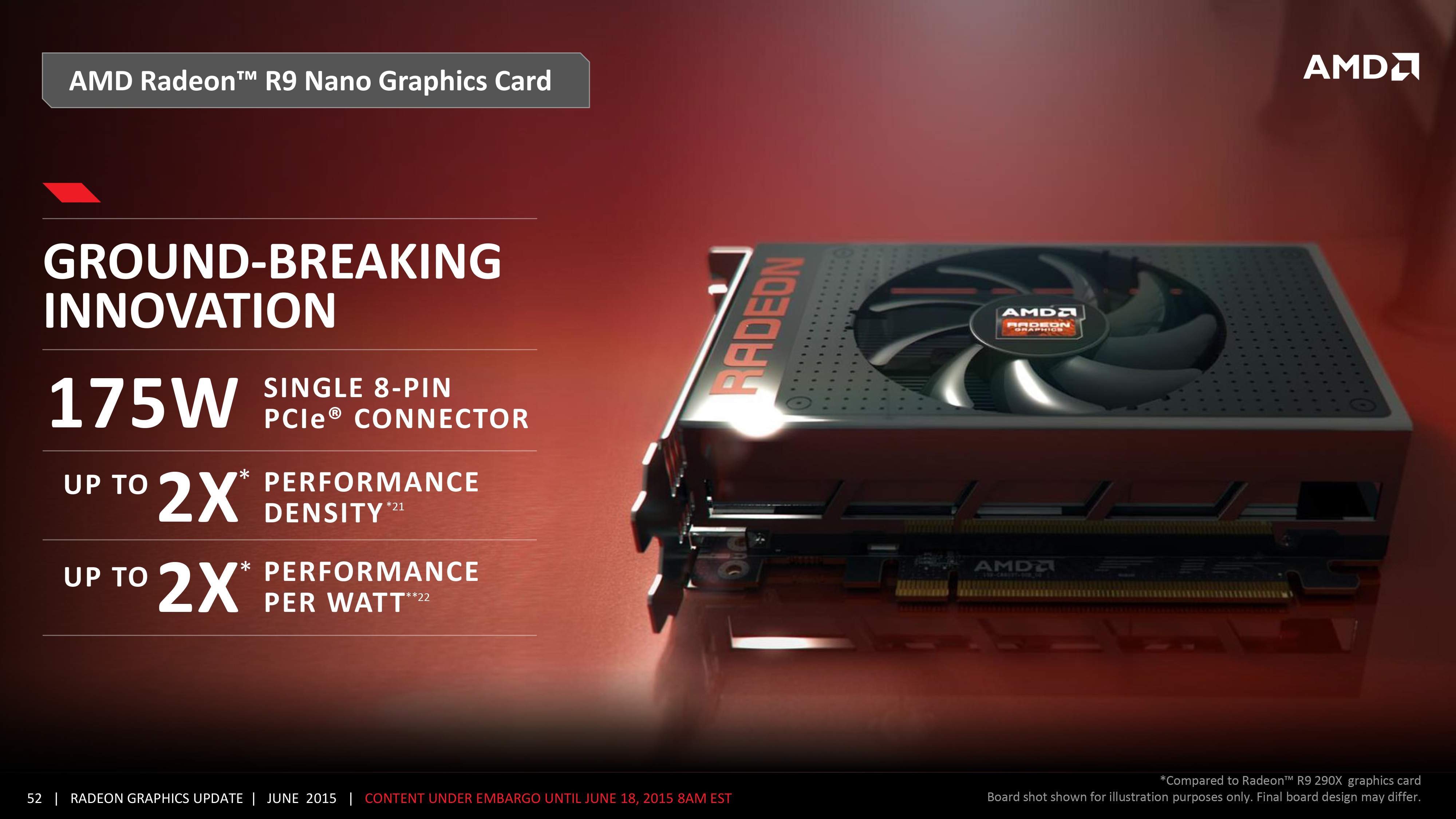
Meanwhile, since R9 Nano’s lower clockspeeds put it closer to the clockspeed/voltage sweet spot than R9 Fury X does, overall power efficiency should be even better than Fury X. AMD is touting that R9 Nano should offer twice the performance per watt of R9 290X, and while R9 290X is not exactly a high point for AMD, this would still be a substaintial improvement for AMD. With the R9 Nano launching at some point this summer, the big unknown here, if anything, will be price. If R9 Nano does end up taking AMD’s best Fiji chips, and given the lack of competition in the small form factor space, it may end up being more expensive than R9 Fury X due to rarity and the performance advantage we’re expecting such a card to have.
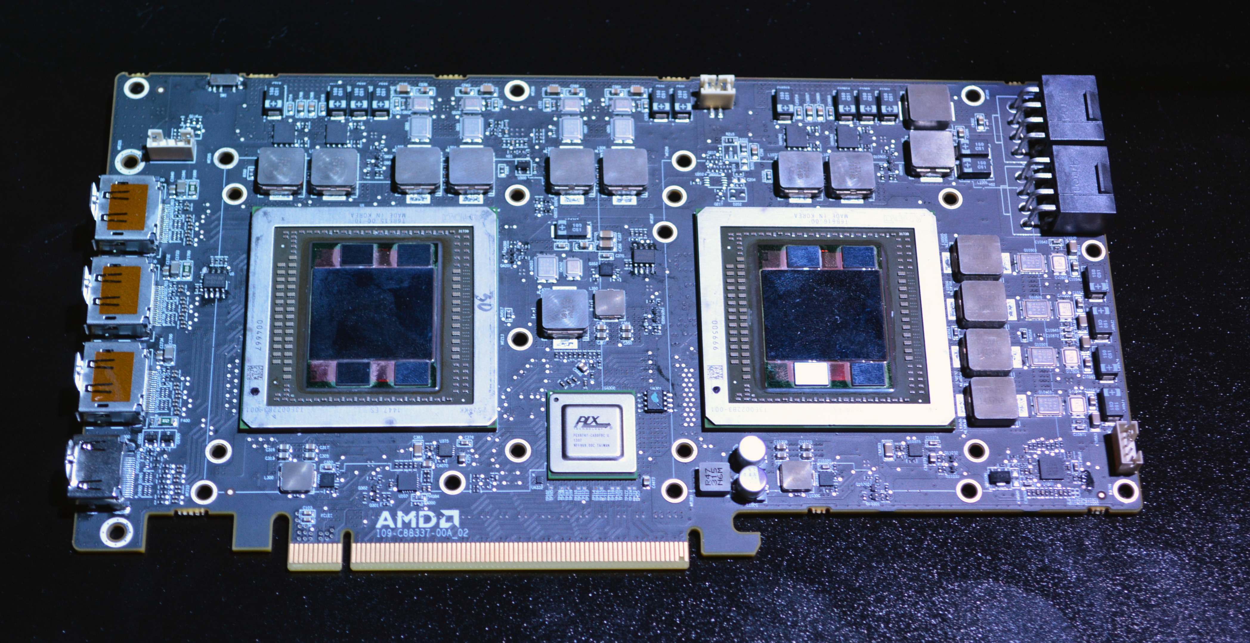
Last but not least in the Fiji lineup will be the company’s unnamed dual GPU card. Quickly teased by AMD CEO Dr. Lisa Su at the PC Gaming Show, the dual-GPU card is already up and running for AMD with an expected launch date of the fall. AMD has not announced specifications or pricing for the card, but they have shown off the naked board, confirming the presence of two Fiji GPUs, along with a pair of 8-pin PCIe power sockets. Meanwhile with 4GB of VRAM for each GPU on-package via HBM technology, AMD has been able to design a dual-GPU card that’s shorter and simpler than their previous dual-GPU cards like the R9 295X2 and HD 7990, saving space that would have otherwise been occupied by GDDR5 memory modules and the associated VRMs.
Based on the Project Quantum sample computers AMD was showing off (more on that in a second), we’re expecting that these will be liquid cooled cards, just like the R9 Fury X. The R9 295X2’s liquid cooler was one of AMD’s big success stories of 2014, delivering excellent cooling and acoustics for what is traditionally a problematic video card design, so it would come as no surprise to see it reused here. The dual GPU card being another 500W card like the R9 295X2 is also a safe bet, but we’ll have to see just what AMD announces in the fall.
Finally, AMD’s last Fiji-related project to come out of the R9 Fury X launch is not another Fiji card, but rather a new PC form factor built around the dual GPU Fiji card. AMD calls this form factor Project Quantum, and it is designed to exploit the size advantage of the Fiji GPU and the non-traditional cooling setups enabled by closed loop liquid coolers.
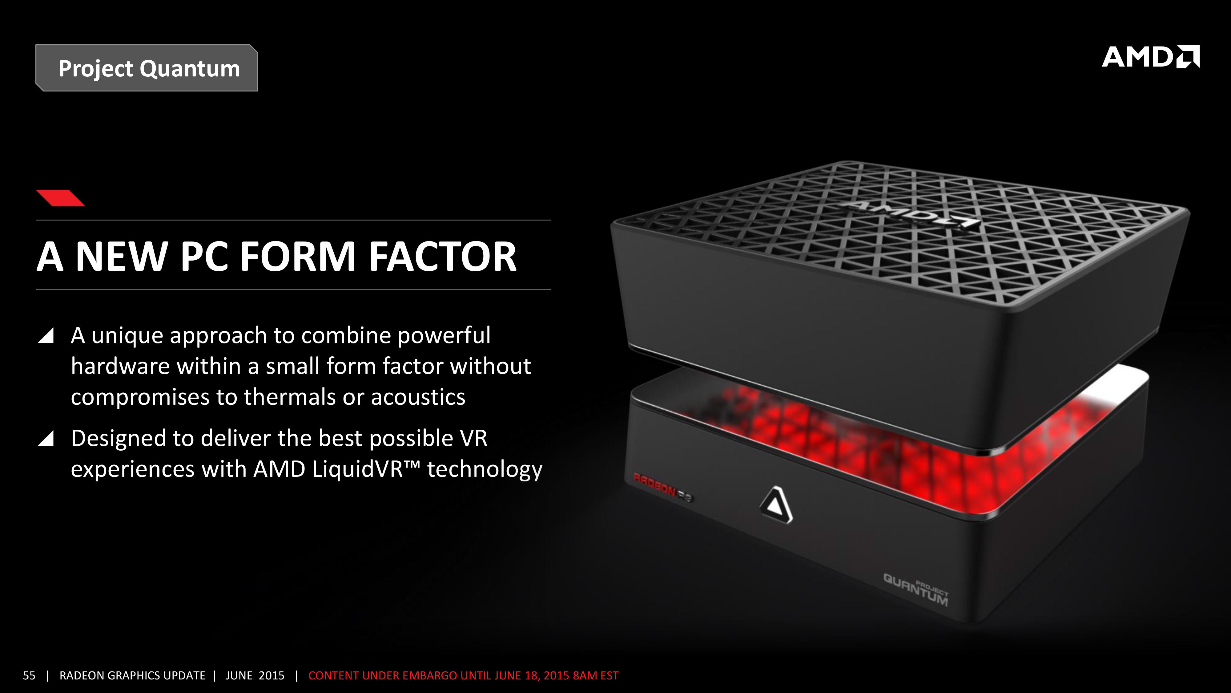
Vaguely resembling a squared-off 1978 Cylon Basestar with its distinct top and bottom halves attached via a narrow tube in the middle, in a Project Quantum computer the lower half of the machine contains all of the electronics while the upper half of the machine contains all of the radiators for the closed loop liquid coolers. Both the Intel CPU and Fiji GPUs are liquid cooled here, so the vast majority of the heat is removed from the lower chamber and directly exhausted out of the top of the machine.
AMD is pitching Project Quantum as an example of the kind of form factors that HBM-equipped GPUs and liquid cooling together can enable, allowing thermal densities greater than traditional, air cooled SFF PCs. The split design in turn is meant to accentuate the fact that all of the electronics at in the bottom chamber, but at the same time there is also a degree of practicality involved since without the split there would be nowhere for the fans to draw air for the top chamber. Finally, since it features a dual GPU card, AMD is also pitching it as a potential VR host design, since VR has high GPU requirements and is expected to scale very well from 1 to 2 GPUs (right eye/left eye).

As for the availability of Project Quantum machines, that much remains to be seen. AMD has made it clear that they don’t intend to sell these machines themselves, and that Project Quantum is a concept, not a product. However if AMD can find a partner to work with to mass produce machines, a retail product similar to Project Quantum is not off the table at this time. Though I suspect even in the best case scenario we’d be looking at 2016 for such retail machines.
Today’s Review: Radeon R9 Fury X
Now that we’ve had a chance to cover all of the architectural and design aspirations of the Fiji GPU and its constituting cards, let’s get down to the business end of this article: the product we’ll be reviewing today.
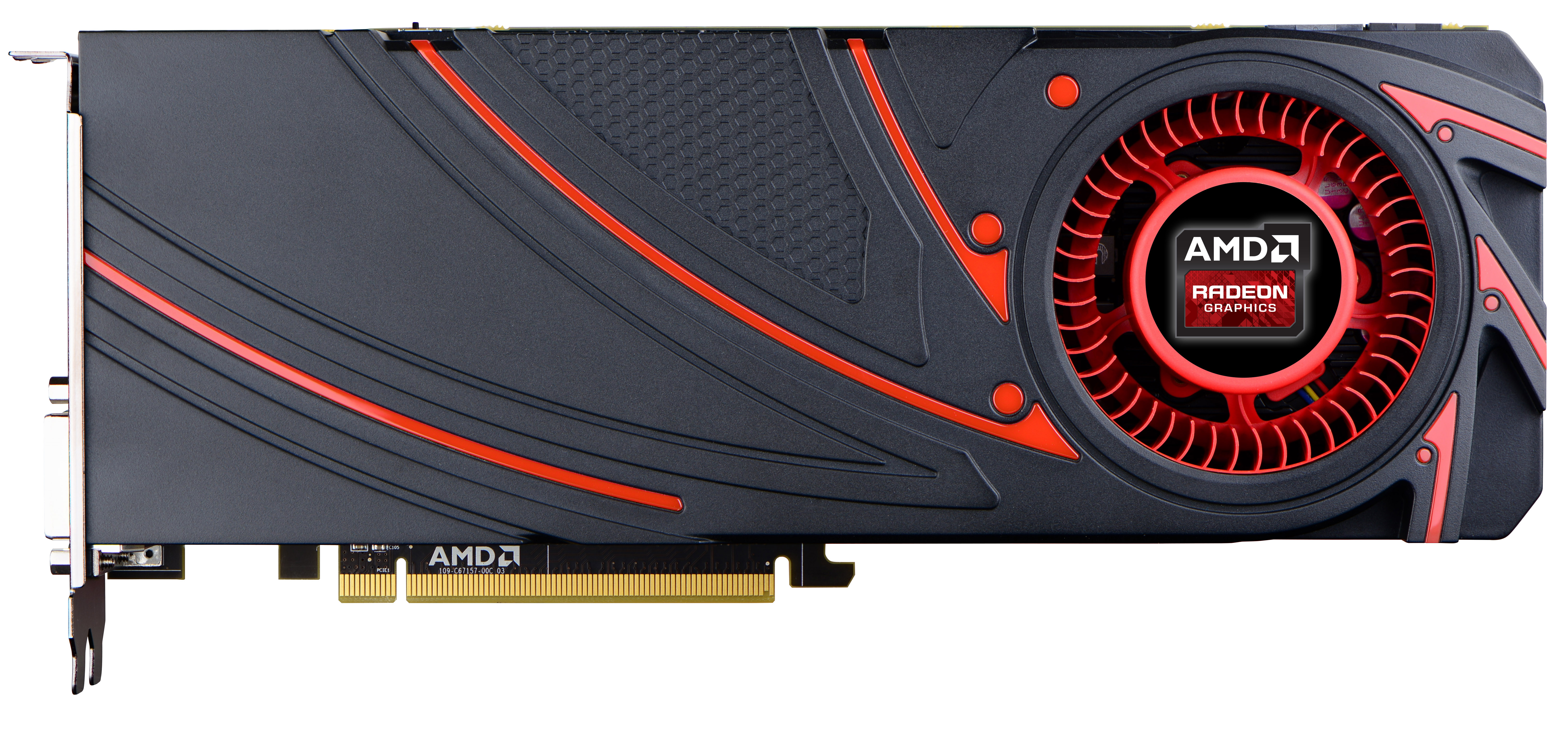
Having launched last week and being reviewed today is AMD’s Radeon R9 Fury X, the company’s new flagship single-GPU video card. Featuring a fully enabled Fiji GPU, the R9 Fury X is Fiji at its finest, and a safe bet to be the grandest video card AMD releases built on TSMC’s 28nm process. Fiji is clocked high, cooled with overkill, and priced to go right up against the only GM200 GeForce card from NVIDIA that anyone cares about: the GeForce GTX 980 Ti.
| AMD GPU Specification Comparison | ||||||
| AMD Radeon R9 Fury X | AMD Radeon R9 Fury | AMD Radeon R9 290X | AMD Radeon R9 290 | |||
| Stream Processors | 4096 | (Fewer) | 2816 | 2560 | ||
| Texture Units | 256 | (How much) | 176 | 160 | ||
| ROPs | 64 | (Depnds) | 64 | 64 | ||
| Boost Clock | 1050MHz | (On Yields) | 1000MHz | 947MHz | ||
| Memory Clock | 1Gbps HBM | (Memory Too) | 5Gbps GDDR5 | 5Gbps GDDR5 | ||
| Memory Bus Width | 4096-bit | 4096-bit | 512-bit | 512-bit | ||
| VRAM | 4GB | 4GB | 4GB | 4GB | ||
| FP64 | 1/16 | 1/16 | 1/8 | 1/8 | ||
| TrueAudio | Y | Y | Y | Y | ||
| Transistor Count | 8.9B | 8.9B | 6.2B | 6.2B | ||
| Typical Board Power | 275W | (High) | 250W | 250W | ||
| Manufacturing Process | TSMC 28nm | TSMC 28nm | TSMC 28nm | TSMC 28nm | ||
| Architecture | GCN 1.2 | GCN 1.2 | GCN 1.1 | GCN 1.1 | ||
| GPU | Fiji | Fiji | Hawaii | Hawaii | ||
| Launch Date | 06/24/15 | 07/14/15 | 10/24/13 | 11/05/13 | ||
| Launch Price | $649 | $549 | $549 | $399 | ||
With a maximum boost clockspeed of 1050MHz and with 4096 SPs organized into 64 CUs, R9 Fury X has been designed to deliver more shading/compute performance than ever before. Hawaii by comparison topped out at 2816 SPs (44 CUs), giving R9 Fury X a 1280 SP (~45%) advantage in raw shading hardware. Meanwhile as a result of scaling up the number of CUs, the number of texture units has also scaled up to 256 texture units, a new high-water mark for the number of texture units in a single GPU from any vendor.
Getting away from the CUs for a second, the R9 Fury X features less dramatic changes at its front-end and back-end relative to Hawaii. Like Hawaii, R9 Fury X features 4 geometry engines on the front-end and 64 ROPs on the back-end, so from a theoretical standpoint Fiji does not have any additional resources to work with on those portions of the rendering pipeline. That said, what the raw specifications do not cover are the architectural optimizations we have covered in past pages, which should see Fiji’s ROPs and geometry engines both perform better per unit and per clock than Hawaii’s. Meanwhile the other significant influence here is the extensive memory bandwidth enabled by using High Bandwidth Memory, which combined with a larger 2MB L2 cache should leave the ROPs far better fed on R9 Fury X than it did on AMD’s Hawaii cards.
As for High Bandwidth Memory, the next-generation memory technology gives AMD more memory bandwidth than ever before. Featuring an ultra-wide 4096-bit memory bus clocked at 1Gbps (500MHz DDR), the R9 Fury X has a whopping 512GB/sec of memory bandwidth, fed by 4GB of HBM organized in 4 stacks of 1GB each. Relative to R9 290X, this represents a 60% increase in memory bandwidth, a true generational jump that we will not see again in an AMD GPU for some number of years to come.
Consequently the performance expectations for R9 Fury X will significantly vary with the nature of the rendering workload. For pure compute workloads, between the 45% increase in SPs and 5% clockspeed increase, R9 Fury X will be up to 53% faster than the R9 290X. Meanwhile for ROP-bound scenarios the difference can be anywhere between 5% and 120%, depending on how bandwidth-bound the task is and how effective delta compression is in shrinking the bandwidth requirements. Real world expectations are 30-40% over R9 290X, depending on the game and the resolution, with R9 Fury X extending its gains at higher resolutions.
For AMD, the Radeon R9 Fury X is a critically important card for a number of reasons. From a technology perspective this is the very first HBM card, and consequently the missteps AMD makes and the lessons they learn here will be important for future generation of cards. At the same time from a competitive perspective, the importance of a flagship cannot be ignored. While flagship card sales are only a tiny part of overall card sales for NVIDIA and AMD, the PC video card industry is (in)famous for its window shopping and the emphasis put on which card holds the performance crown. Most buyers cannot (or will not) buy a card like R9 Fury X, but the sales impact of holding the crown is undeniable, as buyers as a whole will favor whoever can hold the crown. After seeing their consumer discrete market share fall to the lowest level in years, AMD is gunning to get the crown back, and the halo effect that comes from it that spurs on so many additional sales of lower-end cards.

The competition for the R9 Fury X is of course NVIDIA’s recently released GeForce GTX 980 Ti. Based on a cut-down version of NVIDIA’s GM200 GPU, the GTX 980 Ti is an odd card that comes entirely too close to their official flagship GTX Titan X in performance (~95%), to the point where although the GTX Titan X is the de jure flagship for NVIDIA, it is the GTX 980 Ti that is the de facto flagship for the company. Meanwhile, although only NVIDIA knows for sure, given the timing of the GTX 980 Ti’s launch, there is every reason to believe that the company launched it with the specific intent of countering the R9 Fury X before it even launched, so AMD does not enjoy a first-mover advantage here.
Price-wise the R9 Fury X has launched at $649, the same price as the GTX 980 Ti, so between these two cards this is a straight-up fist fight. There is no price spoiler effect in play here, the question simply comes down to which card is the better card. The only advantage for either party in this case is that NVIDIA is offering a free copy of Batman: Arkham Knight with GTX 980 Ti cards, not that the PC port of the game is an asset at this time given its poor state.
Finally, as far as launch quantities are concerned, AMD has declined to comment on how many R9 Fury X cards were available for launch. What we do know is that the cards sold out on the first day and we have yet to see a massive restocking take place yet, though at just a week post-launch restocks typically don’t come quite this soon. In any case whether due to demand, supply, or a mix of the two, the initial launch allocations of R9 Fury X did sell out, and for the moment getting another card is easier said than done.
| Summer 2015 GPU Pricing Comparison | |||||
| AMD | Price | NVIDIA | |||
| Radeon R9 Fury X | $649 | GeForce GTX 980 Ti | |||
| $499 | GeForce GTX 980 | ||||
| Radeon R9 390X | $429 | ||||
| Radeon R9 290X Radeon R9 390 |
$329 | GeForce GTX 970 | |||
| Radeon R9 290 | $250 | ||||
| Radeon R9 380 | $200 | GeFroce GTX 960 | |||
| Radeon R7 370 Radeon R9 270 |
$150 | ||||
| $130 | GeForce GTX 750 Ti | ||||
| Radeon R7 360 | $110 | ||||
Meet The Radeon R9 Fury X
Right off the bat it is safe to say that we have not seen a high-end card quite like the R9 Fury X before. We have seen small cards before, we have seen liquid cooled cards before, and we have seen well-crafted cards before. But none of those attributes have come together before in a single card like they have with the R9 Fury X. AMD has spared no expense on their new single-GPU flagship and it shows.
If we had to describe the R9 Fury X in a nutshell, the only thing that would do it any justice is a very small card with a very big radiator. Liquid cooling is not by any means new (see: R9 295X2), but thanks to the space savings of HBM there hasn’t been a card before that has paired up a small board with a large radiator in this fashion. It is, arguably, a card designed for an entirely different paradigm than the dual-slot air cooled cards we have come to know over the last decade.
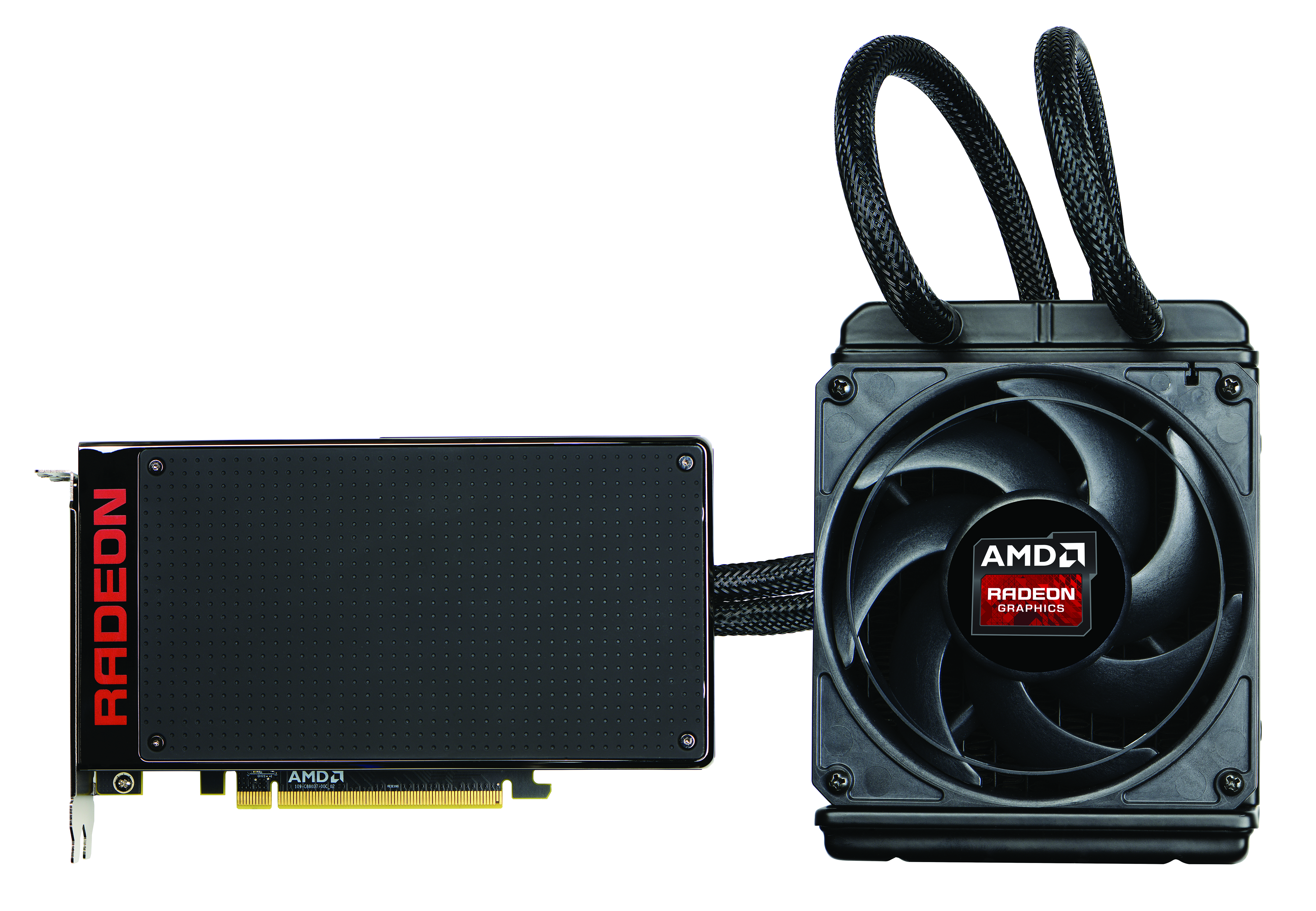
But first, let’s talk about build quality and naming. To cut right to the case, NVIDIA’s initial GTX Titan project saw a large and unexpected amount of success in 2013. Named in honor of the Titan supercomputer, NVIDIA’s first major supercomputer win for their Tesla business, the GTX Titan was created to serve as a new high-end card line for the company. Harkening back to the Titan supercomputer, the GTX Titan created for NVIDIA what amounted to a luxury category for a video card, priced at an unprecedented $1000, but at the same time introducing a level of build quality and performance for a blower-type air cooler that is unmatched to this day. By all reports the GTX Titan handily exceeded NVIDIA’s expectations, and though expensive, established the viability of a higher quality video card.
With the R9 Fury X, AMD is looking to establish the same kind of luxury brand and image for their products. Similar to the Titan, AMD has dropped the number in the product name (though formally we still consider it part of the 300 series), opting instead to brand the product Fury. AMD has not been very clear on the rationale for the Fury name, and while they do not have a high-profile supercomputer to draw a name from, they do have other sources. Depending on what you want to believe the name is either a throwback to AMD’s pre-Radeon (late 1990s) video card lineup, the ATI Rage Fury family. Alternatively, in Greek mythology the Furies were deities of vengeance who had an interesting relationship with the Greek Titans that is completely unsuitable for publication in an all-ages technical magazine, and as such the Fury name may be a dig at NVIDIA’s Titan branding.

In any case, what isn’t in doubt is the quality of the R9 Fury X. AMD has opted to build a card to a similar luxury standard as the GTX Titan, with a focus on both the card and somewhat disembodied radiator. For R9 Fury X AMD has gone metal, and the card proper is composed of a multi-piece die-cast aluminum body that is built around the card’s PCB. While you won’t find any polycarbonate windows here (the pump isn’t exactly eye-catching) what you will find is soft-touch rubber along the front face of the card and its edges. Meanwhile on the back side of the card there is another soft-touch panel to serve as a backplate. Since the card lacks a fan of any kind, there are no cooling concerns here; with or without a backplate, putting R9 Fury X cards side-by-side doesn’t impact cooling in any meaningful manner.
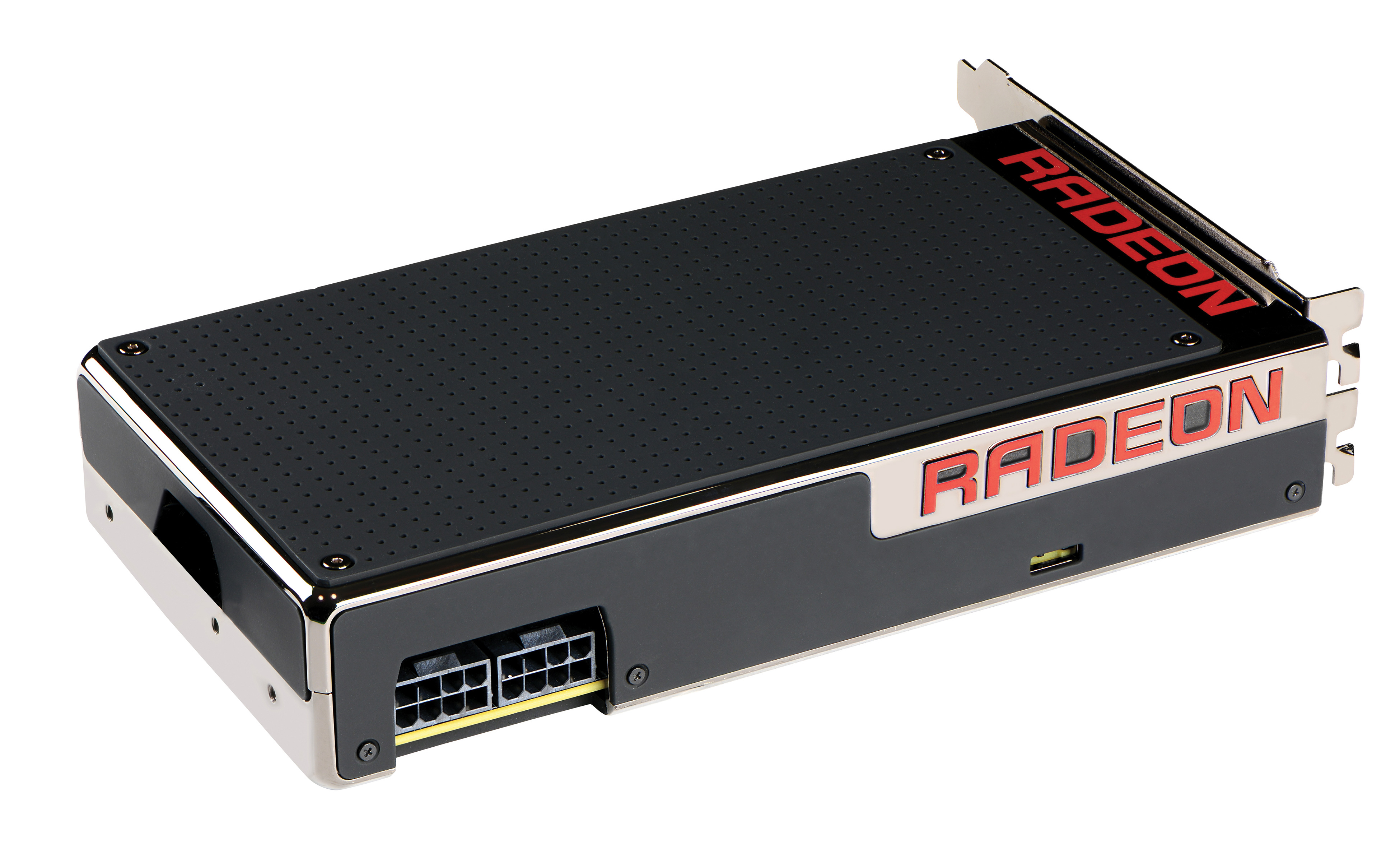
Ultimately at this point AMD and NVIDIA are basically taking cues from the cell phone industry on design, and the end result is a card that looks good, and yes, even feels good in-hand. The R9 Fury X has a very distinctive silhouette to it that should be easily noticeable in any open or windowed case, and in case that fails, you would be hard-pressed to miss the lighting. The card features multiple LED-lit features; the first is the Radeon logo, which lights up red when the card is powered on, and meanwhile directly next to the PCIe power connectors are a bank of LEDs. The LEDs are designed to indicate the load on the card, with 8 LEDs for load, and a final, 9th LED that indicates whether the card has gone until AMD’s ultra-deep sleep ZeroCore Power mode. The 8 load LEDs can even be configured for red or blue operation to color-coordinate with the rest of a case; the only color you can’t select is green, in theory because green is reserved for the sleep LED, though in practice I think it’s safe to point out that green is not AMD’s color…


Moving on, let’s talk about the R9 Fury X’s cooling apparatus, its closed loop liquid cooling system and its rather large radiator. One of AMD’s few success stories in 2014 was the R9 295X2, the company’s dual GPU Hawaii card. After numerous struggles with air cooling for both single and dual GPU cards – R9 290X, Radeon HD 6990, Radeon HD 7990 – and facing a 500W TDP for their Hawaii card, AMD ditched straight air cooling in favor of a closed loop liquid cooler. Though the cooler AMD used was pushed to its limit by the high TDP of the R9 295X2, at the end of the day it did its job and did it well, effectively cooling the card while delivering acoustic performance simply unheard of for a reference dual GPU card.
For the R9 Fury X AMD needs to dissipate over 275W of heat. AMD’s reference cooler for the R9 290X was simply not very good, and even NVIDIA would be hard pressed to dissipate that much heat, as their Titan cooler is optimized around 250W (and things quickly get worse when pushed too far past that). As a result AMD opted to once again go the closed loop liquid cooling (CLLC) route for the R9 Fury X, taking what they learned from the R9 295X2 and improving upon it.

The end result is a bigger, better CLLC that is the only source of cooling for the card. The R9 295X2 used a fan for the VRMs and VRAM, but for the R9 Fury X AMD has slaved everything to the CLLC. The CLLC in turn is even bigger than before; it’s still based around a 120mm radiator, but the combination of radiator and fan is now 60mm thick, and in all honesty the thickest radiator we expect would fit in our closed case testbed. As a result the radiator has an immense 500W rated cooling capability, far outstripping the card’s 275W TBP, and without a doubt making it overkill for the R9 Fury X.
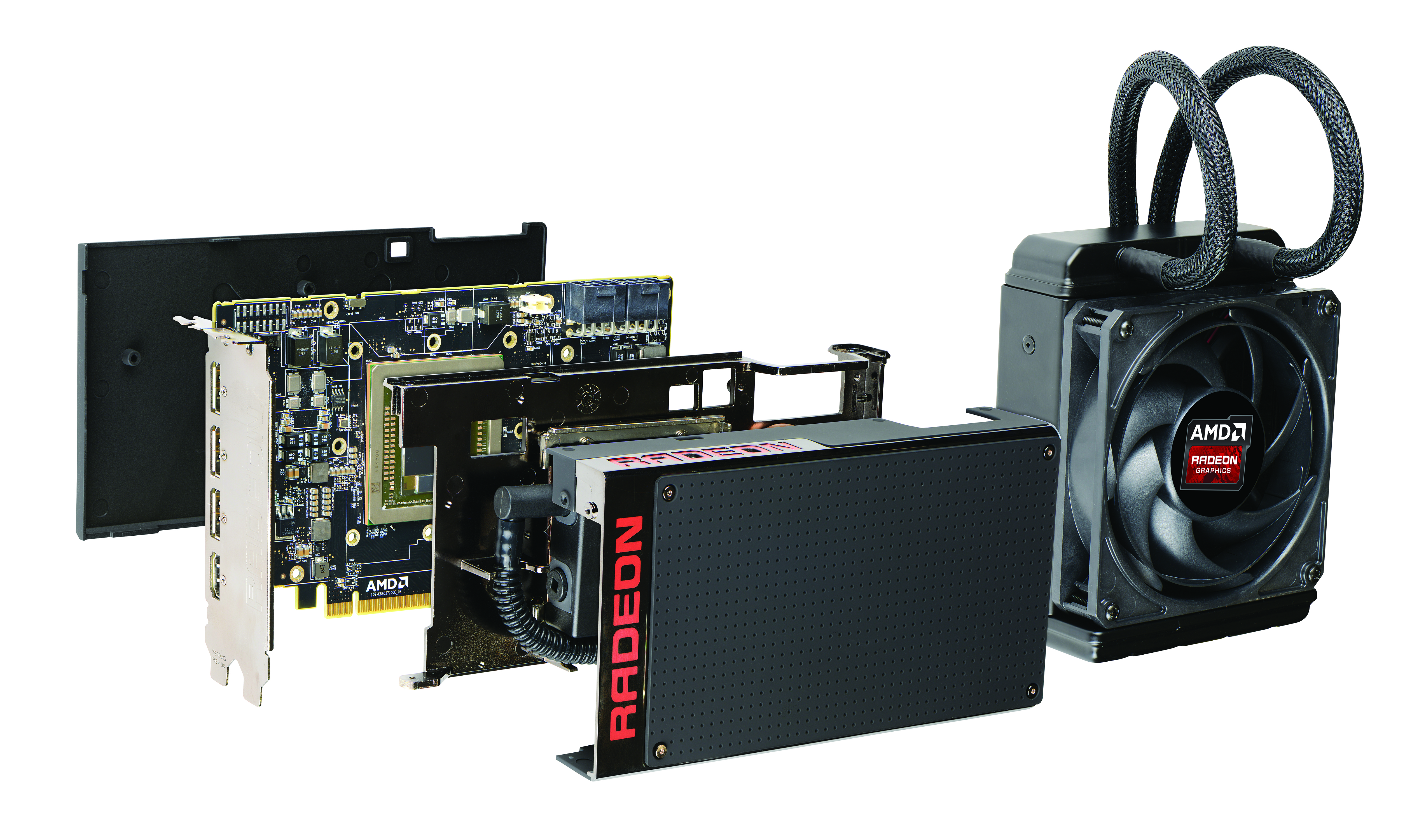
Cracking open the R9 Fury X’s housing to check out the pump block shows us that is built by Cooler Master. Furthermore in order to have the CLLC cool the GPU and supporting discrete components, there is an interesting metal pipe in the loop, which serves as a liquid cooled heatpipe of sorts to draw heat away from the MOSFETs used in the card’s VRM setup. Otherwise the GPU and the HBM modules situated next to it are covered by the pump block itself.

AMD’s official rating for the R9 Fury X’s cooling apparatus is that it should keep the card at 50C while playing games. In practice what we have found is that in our closed case test bed the GPU temperature gets up to 65C, at which point the CLLC fan ramps up very slightly (about another 100RPM) and reaches equilibrium. The low operating temperature of the Fiji GPU is not only a feather in AMD’s cap, but is an important part of the design of the card, as the low temperature keeps power consumption down and improves AMD’s overall energy efficiency.
Meanwhile from an operational standpoint, until the R9 295X2, where the CLLC acted independently based on the temperature of the liquid, the R9 Fury X’s CLLC is slaved into the fan controls for the card. As a result it’s possible for the card (and users) to directly control the fan speed based on GPU/VRM temperatures. The independent CLLC in the R9 295X2 was not a direct problem for that card, but with the CLLC of the R9 Fury X now responsible for the VRMs as well, letting the card control the fan is a must.

Overall the acoustic performance of the R9 Fury X is unprecedented for a high-end card, as we’ll see in our benchmark section. Unfortunately the CLLC does have one drawback, and that is idle noise. Just as with the R9 295X2, there’s no such thing as a free lunch when it comes to moving around coolant, and as a result the pump makes more noise at idle than what you’d find on an air cooled card, be it blower or open air.
Moving on, let’s get back to the card itself. The R9 Fury X ships with an official Typical Board Power (TBP of 275W, this intended to represent the amount of power it will consume during the average gaming session. That said, the power delivery circuitry of the card is designed to deliver quite a bit more energy than that, as the card features a pair of 8-pin PCIe power sockets and has an official power delivery rating of 375W. And although AMD doesn’t specify a board limit in watts, based on empirical testing we were able to get up to an estimated 330W. As a result the card has plenty of power and thermal headroom if desired.

Meanwhile the card’s VRM setup is a 6-phase design. AMD tells us that these VRMs can handle up to 400A, no doubt helped by the liquid cooling taking place. AMD’s out of the box overclocking support is limited – no voltage and no HBM clockspeed controls, only the power limit and GPU clockspeed – but it’s clear that this card was built to take some significant overclocking. To that end there is a dual BIOS switch present that can switch between a programmable BIOS and a fixed reference BIOS, and I can only imagine that AMD is expecting hardcore overclockers to look into BIOS modification to gain the necessary power and voltage controls for more extreme overclocking.
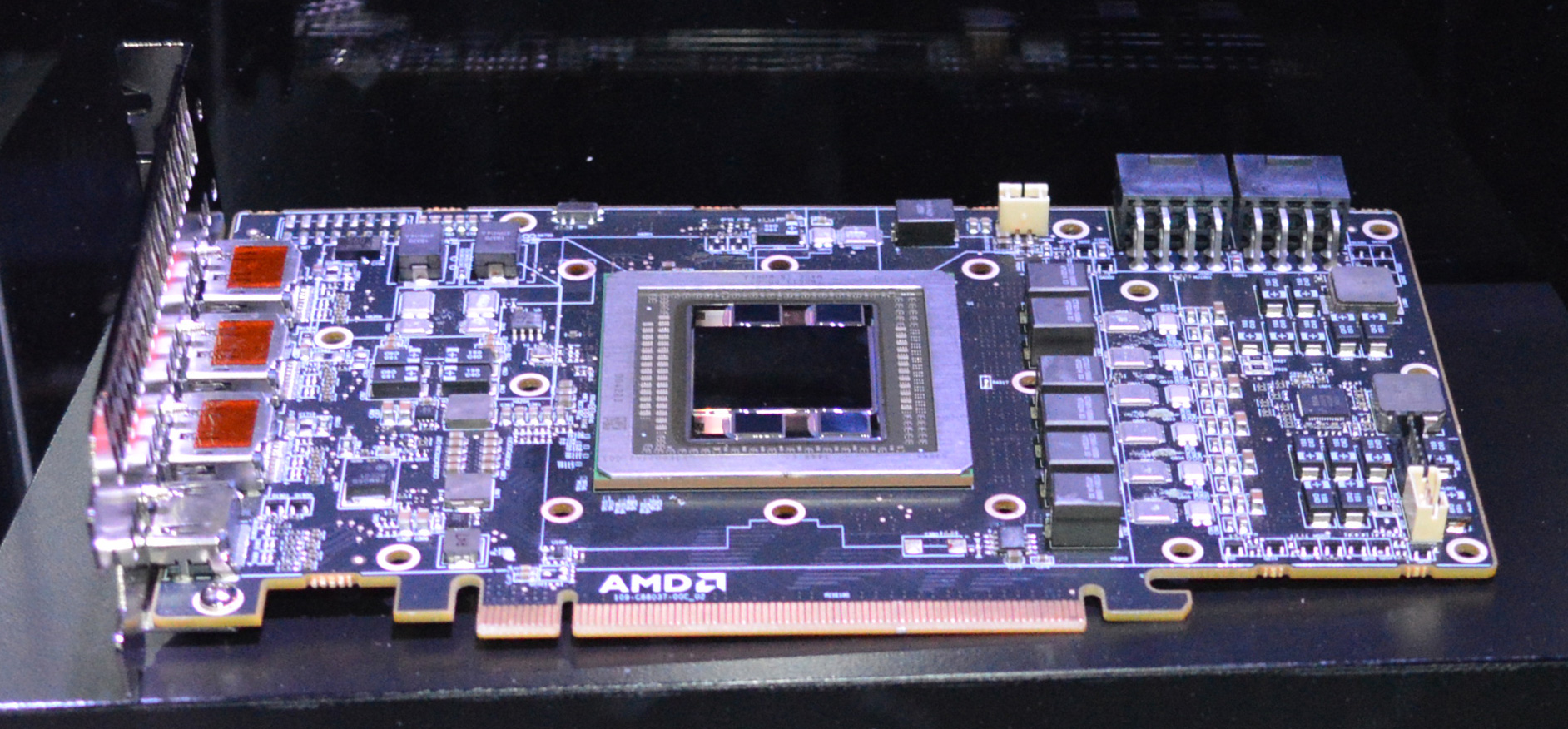
Taking a look at the naked PCB, it’s remarkable how small it is. The PCB measures just 7.5” in length, 3” shorter than the standard 10.5” found on most high-end reference cards. This smaller size is primarily enabled through the use of HBM, which brings the card’s VRAM on-chip and uses relatively tiny stacks of memory as opposed to the large cluster of 16 GDDR5 chips required for R9 290X. HBM also reduces the number of discrete components required for the power delivery system, as HBM has much simpler power delivery requirements. The end result is that a good deal of the board is on the Fiji chip itself, with limited amounts of supporting circuitry forming the rest of the board.
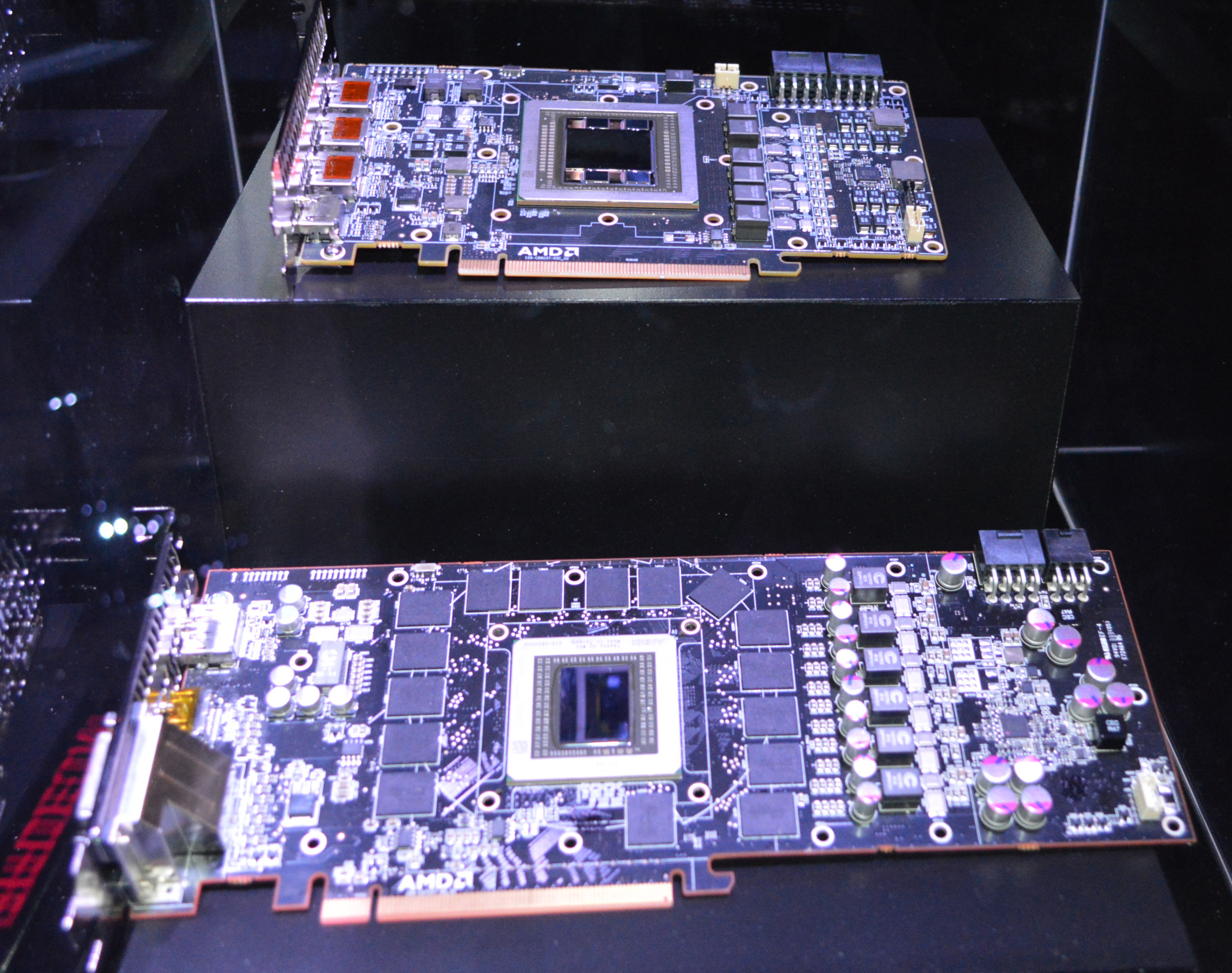
Top: R9 Fury X. Bottom: R9 390X/290X
To show this off, AMD let us take pictures of a bare R9 Fury X PCB next to an R9 290X PCB, and the difference is simply staggering. As a result the R9 Fury X is going to enjoy an interesting niche as a compact, high-performance card. The large radiator does invite certain challenges, but I expect OEM system builders are going to have a fun time designing some Micro-ATX sized SFF PCs around this card.
Switching gears, the Display I/O situation is an interesting one. Without a fan on the card itself, there is no need for vents on the I/O bracket, and as a result we get a solid metal bracket with holes punched out for the card’s 4 display I/O ports. Here we find 3x DisplayPort 1.2a ports, and a single HDMI 1.4a port. What you will not find is a DL-DVI port; after going down to 1 port on Radeon HD 7970 and back to 2 ports on the Radeon R9 290X, AMD has eliminated the port entirely. Physically I believe this to be based on the fact that the size of the card combined with the pump doesn’t leave room for a DVI port on the second row, though I will also note that AMD announced a few years ago that they were targeting a 2015 date to begin removing DVI ports.
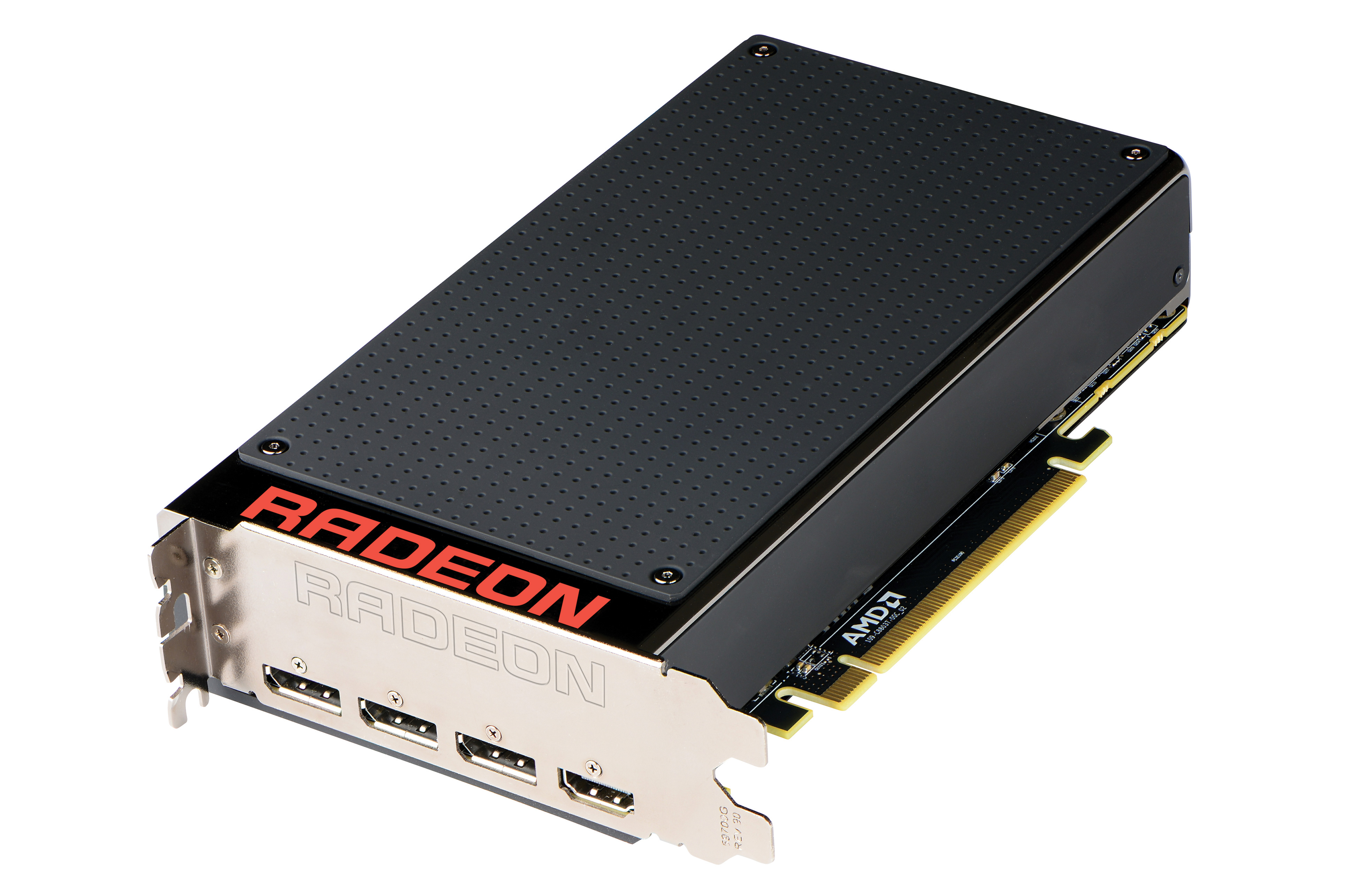
What this means is that the R9 Fury X can natively only drive newer DisplayPort and HDMI equipped monitors. While DVI-only monitors are rare in 2015 (essentially everything has an HDMI port), owners of only DVI-only monitors will be in an interesting situation. With DisplayPort AMD has plenty of flexibility – it can essentially be converted to anything with the right adapter – so owners of DVI-only monitors would either need a cheap passive DP-to-SL-DVI adapter for single link DVI monitors, while they will need a more expensive DP-to-DL-DVI adapter for dual link DVI monitors. Cutting off DVI users was always going to be hard and R9 Fury X doesn’t make it any easier, but on the other hand there’s no getting around the fact that the DVI connector is large, outdated, and space-inefficient in 2015.
Wrapping things up, as far as build quality goes the R9 Fury X is without a doubt the best designed reference Radeon card to date. AMD has learned quite a bit from the R9 290X, and while there is a balance of factors in play here, there is no question that AMD has addressed the build quality issues of their past reference cards in a big way. We have moved on from the late 2000s and early 2010s, and the days of cards like the GTX 280, GTX 480, Radeon HD 6990, and Radeon R9 290X should be behind us. PC video cards, even high-end cards, do not and should not need to be that noisy ever again.
With that said, I do have some general concerns about the fact that the only cards to ship with a high-clocked fully-enabled Fiji GPU will be liquid cooled. Until now air cooling has always been the baseline and liquid cooling the niche alternative, and while I strongly favor quieter cards, there is none the less the question about what it means when AMD tells us that R9 Fury X will only be available with liquid cooling. After the limits of air cooling put a lid on GPU power consumption, will the switch to a CLLC by AMD usher in a new war of power, where everyone is able to once again ramp up power consumption thanks to the greater cooling capabilities of a CLLC?
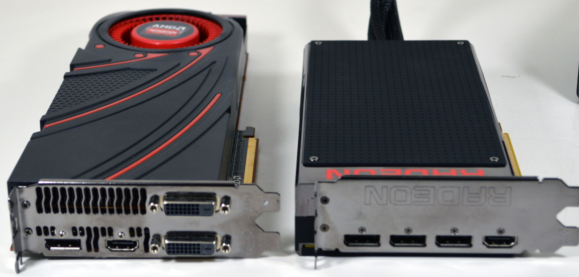
In the meantime AMD considers the CLLC to be an advantage for them, not just for technical reasons but for marketing reasons. The bill of materials cost on the CLLC is quite high – likely around $80 even in volume for AMD – so don’t be surprised to see if AMD includes that on their cost calculus when promoting the card. They spent the money on a more effective cooler, and they want buyers to know that this is a cost baked in to the base price of the card.
That said, it’s important here to note that this is nothing NVIDIA couldn’t replicate if they really wanted to. Their partners already sell CLLC cards as premium cards, which means AMD has to tread carefully here as NVIDIA could easily go CLLC at a lower price and erase AMD’s advantage, though not without taking a hit to their margins (something I suspect AMD would be just fine with).
Finally, as we’ve already hashed out the implications of 4GB of VRAM a few pages back when addressing the 4GB question, we won’t repeat ourselves in length here. But in summary, while 4GB of VRAM is enough for now, it is only just. The R9 Fury X is likely to face VRAM pressure in under 2 years.
The State of Mantle, The Drivers, & The Test
Before diving into our long-awaited benchmark results, I wanted to quickly touch upon the state of Mantle now that AMD has given us a bit more insight into what’s going on.
With the Vulkan project having inherited and extended Mantle, Mantle’s external development is at an end for AMD. AMD has already told us in the past that they are essentially taking it back inside, and will be using it as a platform for testing future API developments. Externally then AMD has now thrown all of their weight behind Vulkan and DirectX 12, telling developers that future games should use those APIs and not Mantle.
In the meantime there is the question of what happens to existing Mantle games. So far there are about half a dozen games that support the API, and for these games Mantle is the only low-level API available to them. Should Mantle disappear, then these games would no longer be able to render at such a low-level.
The situation then is that in discussing the performance results of the R9 Fury X with Mantle, AMD has confirmed that while they are not outright dropping Mantle support, they have ceased all further Mantle optimization. Of particular note, the Mantle driver has not been optimized at all for GCN 1.2, which includes not just R9 Fury X, but R9 285, R9 380, and the Carrizo APU as well. Mantle titles will probably still work on these products – and for the record we can’t get Civilization: Beyond Earth to play nicely with the R9 285 via Mantle – but performance is another matter. Mantle is essentially deprecated at this point, and while AMD isn’t going out of their way to break backwards compatibility they aren’t going to put resources into helping it either. The experiment that is Mantle has come to an end.
This will in turn impact our testing somewhat. For our 2015 benchmark suite we began using low-level APIs when available, which in the current game suite includes Battlefield 4, Dragon Age: Inquisition, and Civilization: Beyond Earth, not counting on AMD to cease optimizing Mantle quite so soon. As a result we’re in the uncomfortable position of having to backtrack on our policies some in order to not base our recommendations on stupid settings.
Starting with this review we’re going to use low-level APIs when available, and when using them makes performance sense. That means we’re not going to use Mantle in the cases where performance has clearly regressed due to a lack of optimizations, but will use it for games where it still works as expected (which essentially comes down to Civ: BE). Ultimately everything will move to Vulkan and DirectX 12, but in the meantime we will need to be more selective about where we use Mantle.
The Drivers
For the launch of the 300/Fury series, AMD has taken an unexpected direction with their drivers. The launch driver for these parts is the Catalyst 15.15 driver, AMD’s next major driver branch which includes everything from Fiji support to WDDM 2.0 support. However in launching these parts, AMD has bifurcated their drivers; the new cards get Catalyst 15.15, the old cards get Catalyst 15.6 (driver version 14.502).
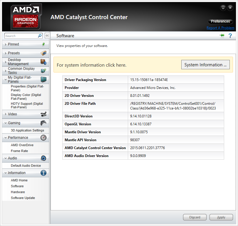
Eventually AMD will bring these cards back together in a later driver release, after they have done more extensive QA against their older cards. In the meantime it’s possible to use a modified version of Catalyst 15.15 to enable support for some of these older cards, but unsigned drivers and Windows do not get along well, and it introduces other potential issues. Otherwise considering that these new drivers do include performance improvements for existing cards, we are not especially happy with the current situation. Existing Radeon owners are essentially having performance held back from them, if only temporarily. Small tomes could be written on AMD’s driver situation – they clearly don’t have the resources to do everything they’d like to at once – but this is perhaps the most difficult situation they’ve put Radeon owners in yet.
The Test
Finally, let’s talk testing. For our benchmarking we have used AMD’s Catalyst 15.15 beta drivers for the R9 Fury X, and their Catalyst 15.5 beta drivers for all other AMD cards. Meanwhile for NVIDIA cards we are on release 352.90.
From a build standpoint we’d like to remind everyone that installing a GPU radiator in our closed cased test bed does require reconfiguring the test bed slightly; a 120mm rear exhaust fan must be removed to make room for the GPU radiator.
| CPU: | Intel Core i7-4960X @ 4.2GHz |
| Motherboard: | ASRock Fatal1ty X79 Professional |
| Power Supply: | Corsair AX1200i |
| Hard Disk: | Samsung SSD 840 EVO (750GB) |
| Memory: | G.Skill RipjawZ DDR3-1866 4 x 8GB (9-10-9-26) |
| Case: | NZXT Phantom 630 Windowed Edition |
| Monitor: | Asus PQ321 |
| Video Cards: | AMD Radeon R9 Fury X AMD Radeon R9 295X2 AMD Radeon R9 290X AMD Radeon R9 285 AMD Radeon HD 7970 NVIDIA GeForce GTX Titan X NVIDIA GeForce GTX 980 Ti NVIDIA GeForce GTX 980 NVIDIA GeForce GTX 780 Ti NVIDIA GeForce GTX 680 NVIDIA GeForce GTX 580 |
| Video Drivers: | NVIDIA Release 352.90 Beta AMD Catalyst Cat 15.5 Beta (All Other AMD Cards) AMD Catalyst Cat 15.15 Beta (R9 Fury X) |
| OS: | Windows 8.1 Pro |
Battlefield 4
Kicking off our benchmark suite is Battlefield 4, DICE’s 2013 multiplayer military shooter. After a rocky start, Battlefield 4 has since become a challenging game in its own right and a showcase title for low-level graphics APIs. As these benchmarks are from single player mode, based on our experiences our rule of thumb here is that multiplayer framerates will dip to half our single player framerates, which means a card needs to be able to average at least 60fps if it’s to be able to hold up in multiplayer.
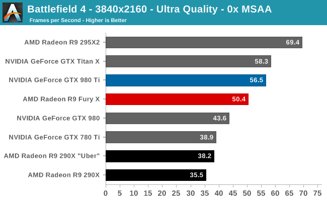
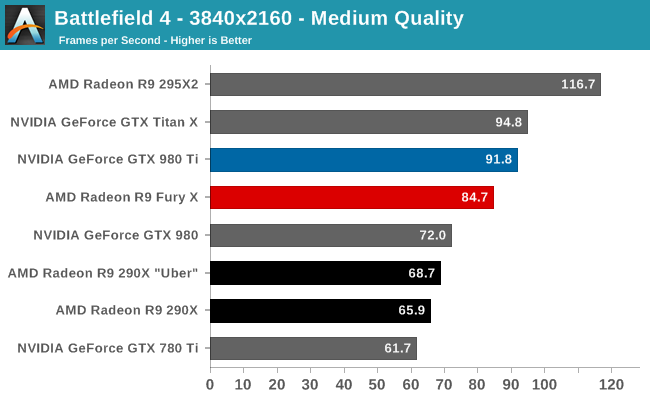
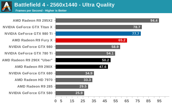
As we briefly mentioned in our testing notes, our Battlefield 4 testing has been slightly modified as of this review to accommodate the changes in how AMD is supporting Mantle. This benchmark still defaults to Mantle for GCN 1.0 and GCN 1.1 cards (7970, 290X), but we’re using Direct3D for GCN 1.2 cards like the R9 Fury X. This is due to the lack of Mantle driver optimizations on AMD’s part, and as a result the R9 Fury X sees poorer performance here, especially at 2560x1440 (65.2fps vs. 54.3fps).
In any case, regardless of the renderer you pick, our first test does not go especially well for AMD and the R9 Fury X. The R9 Fury X does not take the lead at any resolution, and in fact this is one of the worse games for the card. At 4K AMD trails by 8-10%, and at 1440p that’s 16%. In fact the latter is closer to the GTX 980 than it is the GTX 980 Ti. Even with the significant performance improvement from the R9 Fury X, it’s not enough to catch up to NVIDIA here.
Meanwhile the performance improvement over the R9 290X “Uber” stands at between 23% and 32% depending on the resolution. AMD not only scales better than NVIDIA with higher resolutions, but R9 Fury X is scaling better than R9 290X as well.
Crysis 3
Still one of our most punishing benchmarks, Crysis 3 needs no introduction. With Crysis 3, Crytek has gone back to trying to kill computers and still holds the “most punishing shooter” title in our benchmark suite. Only in a handful of setups can we even run Crysis 3 at its highest (Very High) settings, and that’s still without AA. Crysis 1 was an excellent template for the kind of performance required to drive games for the next few years, and Crysis 3 looks to be much the same for 2015.
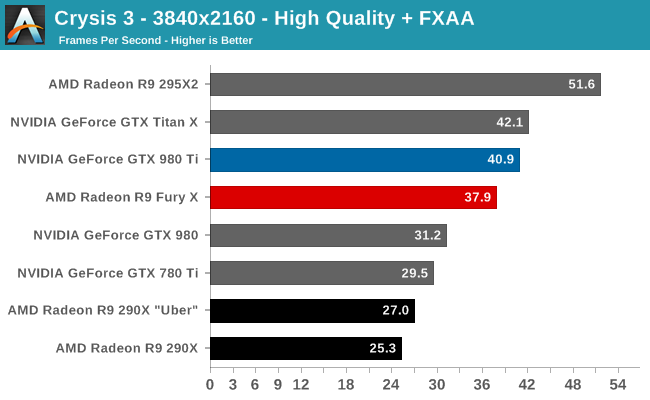
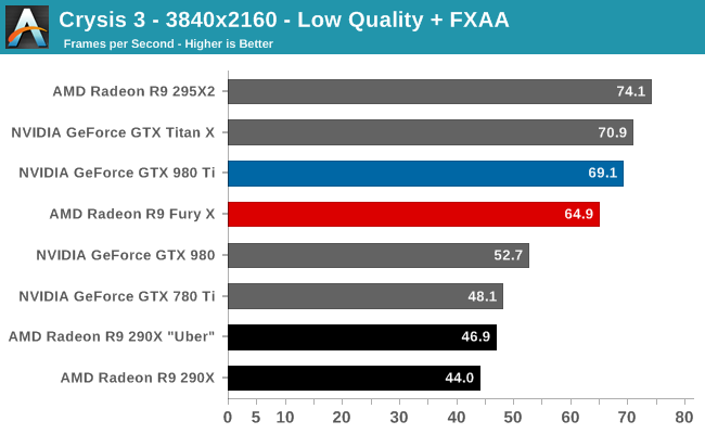
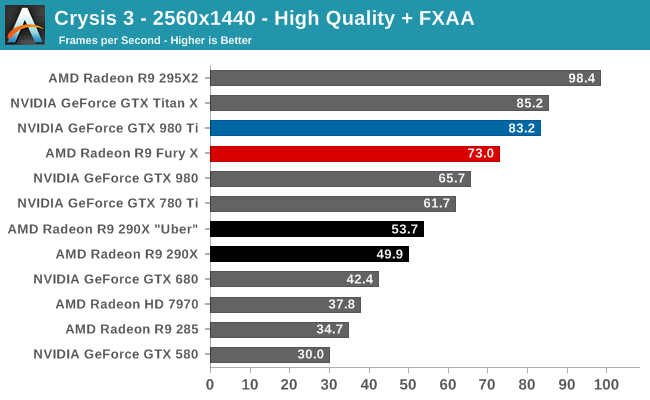
A pure and strenuous DirectX 11 test, Crysis 3 in this case is a pretty decent bellwether for the overall state of the R9 Fury X. Once again the card trails the GTX 980 Ti, but not by quite as much as we saw in Battlefield 4. In this case the gap is 6-7% at 4K, and 12% at 1440p, not too far off of 4% and 10% respectively. This test hits the shaders pretty hard, so of our tried and true benchmarks I was expecting this to be one of the better games for AMD, so the results in a sense do end up as surprising.
In any case, on an absolute basis this is also a good example of the 4K quality tradeoff. R9 Fury X is fast enough to deliver 1440p at high quality settings over 60fps, or 4K with reduced quality settings over 60fps. Otherwise if you want 4K with high quality settings, the performance hit means a framerate average in just the 30s.
Otherwise the gains over the R9 290XU are quite good. The R9 Fury X picks up 38-40% at 4K, and 36% at 1440p. This trends relatively close to our 40% expectations for the card, reinforcing just how big of a leap the card is for AMD.
Middle Earth: Shadow of Mordor
Our next benchmark is Monolith’s popular open-world action game, Middle Earth: Shadow of Mordor. One of our current-gen console multiplatform titles, Shadow of Mordor is plenty punishing on its own, and at Ultra settings it absolutely devours VRAM, showcasing the knock-on effect of current-gen consoles have on VRAM requirements.
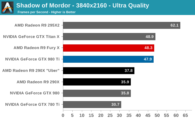
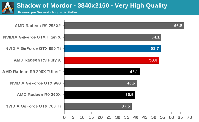
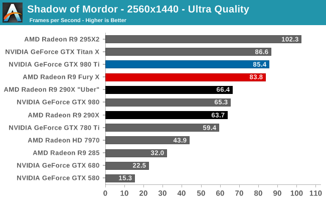
With Shadow of Mordor things finally start looking up for AMD, as the R9 Fury X scores its first win. Okay, it’s more of a tie than a win, but it’s farther than the R9 Fury X has made it so far.
At 4K with Ultra settings the R9 Fury X manages an average of 48.3fps, a virtual tie with the GTX 980 Ti and its 47.9fps. Dropping down to Very High quality does see AMD pull back just a bit, but with a difference between the two cards of just 0.7fps, it’s hardly worth worrying about. Even 2560 looks good for AMD here, trailing the GTX 980 Ti by just over 1fps, at an average framerate of over 80fps. Overall the R9 Fury X delivers 98% to 101% of the performance of the GTX 980 Ti, more or less tying the direct competitor to AMD’s latest card.
Meanwhile compared to the R9 290X, the R9 Fury X doesn’t see quite the same gains. Performance is a fairly consistent 26-28% ahead of the R9 290X, less than what we’ve seen elsewhere. Earlier we discussed how the R9 Fury X’s performance gains will depend on which part of the GPU is getting stressed the most; tasks that stress the shaders show the most gains, and tasks that stress geometry or the ROPs potentially show the lowest gains. In the case of SoM, I believe we’re seeing at least a partial case of being geometry/ROP influenced.
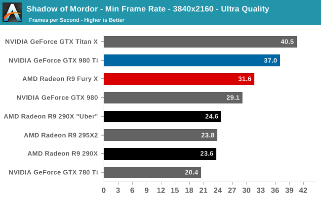
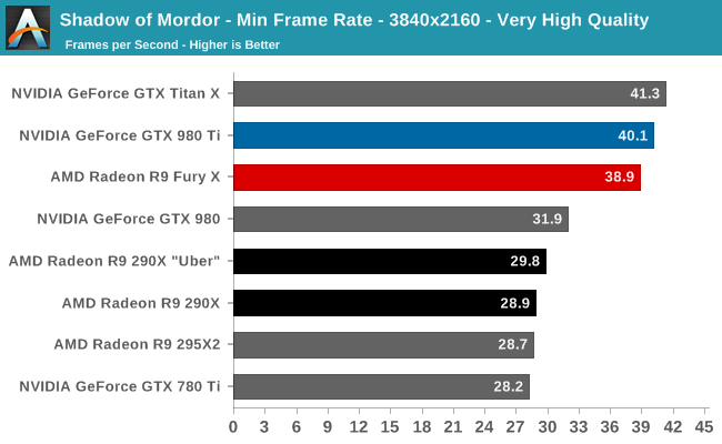
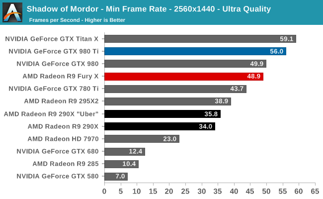
Unfortunately for AMD, the minimum framerate situation isn’t quite as good as the averages. These framerates aren’t bad – the R9 Fury X is always over 30fps – but even accounting for the higher variability of minimum framerates, they’re trailing the GTX 980 Ti by 13-15% with Ultra quality settings. Interestingly at 4K with Very High quality settings the minimum framerate gap is just 3%, in which case what we are most likely seeing is the impact of running Ultra settings with only 4GB of VRAM. The 4GB cards don’t get punished too much for it, but for R9 Fury X and its 4GB of HBM, it is beginning to crack under the pressure of what is admittedly one of our more VRAM-demanding games.
Civilization: Beyond Earth
Shifting gears from action to strategy, we have Civilization: Beyond Earth, the latest in the Civilization series of strategy games. Civilization is not quite as GPU-demanding as some of our action games, but at Ultra quality it can still pose a challenge for even high-end video cards. Meanwhile as the first Mantle-enabled strategy title Civilization gives us an interesting look into low-level API performance on larger scale games, along with a look at developer Firaxis’s interesting use of split frame rendering with Mantle to reduce latency rather than improving framerates.
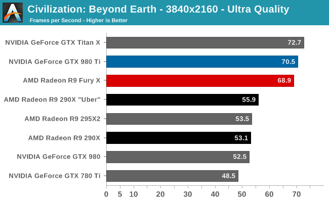
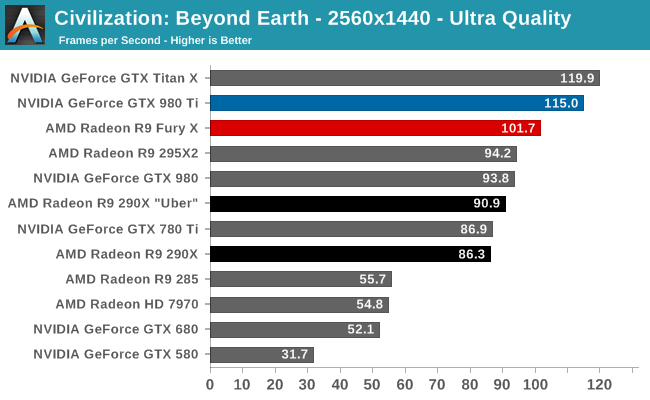
Unlike Battlefield 4 where we needed to switch back to DirectX for performance reasons on the R9 Fury X, AMD’s latest card still holds up rather well on Mantle here, probably due to the fact that Civilization is a newer game. Though not drawn in this chart, what we find is that AMD loses a frame or two per second for running Mantle, but in return they see far, far better minimums (more on that later).
Overall then the R9 Fury X looks pretty good at 4K. Even at Ultra quality it can deliver a better than 60fps average and is within 2% of the GTX 980 Ti. On the other hand AMD struggles a bit more at 1440p, where the absolute framerate is still rather high, but relative to the GTX 980 Ti it’s now an 11% performance gap. This being a Mantle game, the fact that AMD does fall behind is a bit surprising, as at a high level they should be enjoying the CPU benefits of the low-level API. We’ll revisit 1440p performance a bit later on, but this is going to be a recurring quirk for AMD, and a detriment for 1440p 144Hz monitor owners.
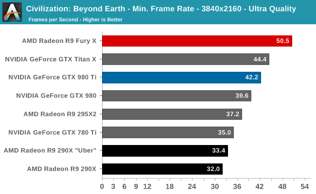
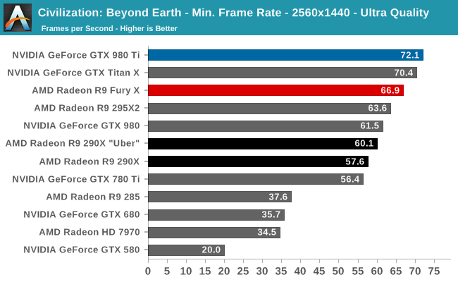
The bigger advantage of Mantle is really the minimum framerates, and here the R9 Fury X soars. At 4K the R9 Fury X delivers a minimum framerate of 50.5fps, some 20% better than the GTX 980 Ti. Both cards do well enough here, but it goes without saying that this is a very distinct difference, and one that is well in AMD’s favor. The only downside for AMD here is that they can’t keep this advantage at 1440p, where they go back to trailing the GTX 980 Ti in minimum framerates by 7%.
On that note I do have one concern here with AMD’s support plans for Mantle. Mainly I’m worried that as well as the R9 Fury X does here, there’s a risk Mantle may stop working in the future. The GCN 1.2 based R9 285 can’t use the Mantle path at all (it crashes), and the R9 Fury X is not all that different in architecture.
Dragon Age: Inquisition
Our RPG of choice for 2015 is Dragon Age: Inquisition, the latest game in the Dragon Age series of ARPGs. Offering an expansive world that can easily challenge even the best of our video cards, Dragon Age also offers us an alternative take on EA/DICE’s Frostbite 3 engine, which powers this game along with Battlefield 4.
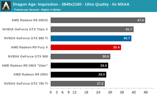
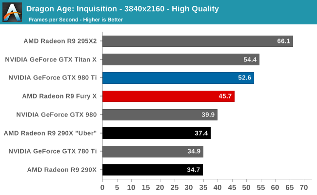
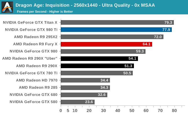
Similar to Battlefield 4, we have swapped out Mantle for DirectX here; the R9 Fury X didn’t suffer too much from Mantle, but it certainly was not in the card’s favor.
Perhaps it’s a Frostbite thing or maybe AMD just got unlucky here, but Dragon Age is the second-worst showing for the R9 Fury X. The card trails the GTX 980 Ti at all times, by anywhere between 13% and 18%. At this point AMD is straddling the line between the GTX 980 and GTX 980 Ti, and at 1440p they fall closer to the GTX 980.
Meanwhile I feel this is another good example of why single-GPU cards aren’t quite ready yet for no-compromises 4K gaming. Even without MSAA the R9 Fury X can’t break out of the 30s, we have to drop to High quality to do that. On the other hand going to 1440p immediately gets Ultra quality performance over 60fps.
Finally, the R9 Fury X’s performance gains over its predecessor are also among their lowest here. The Fiji based card picks up just 22% at 4K, and less at 1440p. Once again we are likely looking at a bottleneck closer to geometry or ROP performance, which leaves the shaders underutilized.
The Talos Principle
Croteam’s first person puzzle and exploration game The Talos Principle may not involve much action, but the game’s lush environments still put even fast video cards to good use. Coupled with the use of 4x MSAA at Ultra quality, and even a tranquil puzzle game like Talos can make a good case for more powerful video cards.
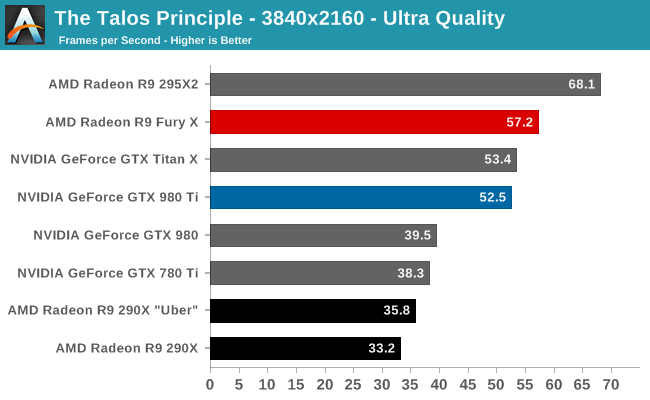
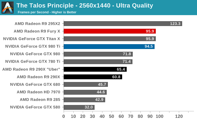
Coming off of AMD’s poor Dragon Age performance, The Talos Principle offers the R9 Fury X a much-needed win. At 4K with Ultra quality settings the card is able to hit 57.2fps, just shy of 60fps. More importantly it’s ahead of not only the GTX 980 Ti, but the GTX Titan X as well, taking down both of NVIDIA’s flagships at once. The 9% lead over the GTX 980 Ti is one of the best AMD will see all day, so this is a game that’s clearly in AMD’s favor.
Do note however that AMD’s performance once again regresses at 1440p. It’s enough to retain the lead, if just barely, and tie the GTX Titan X. Thankfully for AMD this is an example of a game where a single GPU card is plenty for 4K gaming.
As for the R9 290X comparison, the results end up being very interesting. The R9 Fury X sees some very impressive gains here, improving over the R9 290X by 47% at 1440p and an amazing 60% at 4K. Given that the latter is outright outside our theoretical performance window for a shader-bound scenario, I suspect there’s more at play here than just GPU improvements. And sure enough, running the modified Catalyst 15.15 drivers on the R9 290X finds that performance improves by 21% at 4K, to 43.6fps, so it looks like AMD has been doing some optimizing for this game.
Far Cry 4
The next game in our 2015 GPU benchmark suite is Far Cry 4, Ubisoft’s Himalayan action game. A lot like Crysis 3, Far Cry 4 can be quite tough on GPUs, especially with Ultra settings thanks to the game’s expansive environments.
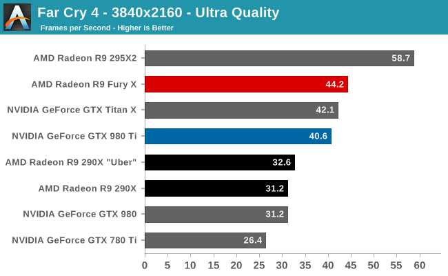

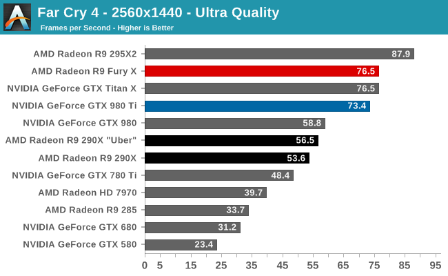
Like the Talos Principle, this is another game that treats AMD well. The R9 Fury X doesn’t just beat the GTX 980 Ti at 4K Ultra, but it beats the GTX Titan X as well. Even 1440p Ultra isn’t too shabby, with a smaller gap but none the less the same outcome.
Overall what we find is that the R9 Fury X has a 9% lead at 4K Ultra, and a 4% lead at 1440p Ultra, making this one of the only games where AMD takes the lead at 1440p. However something interesting happens if we run at 4K with lower quality settings, and that lead evaporates very quickly, shifting to an NVIDIA lead by roughly the same amount. At this time I don’t have a good explanation for this other than to say that whatever is going on at Ultra, it clearly is very different from what happens at Medium quality, and it favors AMD.
Finally, the performance gains over the R9 290X are around average. At 4K and 1440p Ultra the R9 Fury X picks up 35%; at 4K Medium that shrinks to 30%.
Total War: Attila
The second strategy game in our benchmark suite, Total War: Attila is the latest game in the Total War franchise. Total War games have traditionally been a mix of CPU and GPU bottlenecks, so it takes a good system on both ends of the equation to do well here. In this case the game comes with a built-in benchmark that plays out over a large area with a fortress in the middle, making it a good GPU stress test.
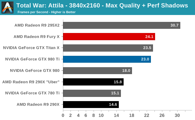
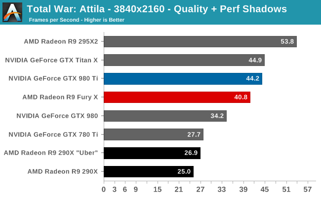
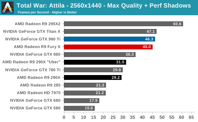
Attila is the third win in a row for AMD at 4K. Here the R9 Fury X beats the GTX 980 Ti by 5% at the Max quality setting. However as this benchmark is very forward looking (read: ridiculously GPU intensive), the actual performance at 4K Max isn’t very good. No single GPU card can average 30fps here, and framerates will easily dip below 20fps. Since this is a strategy game we don’t have the same high bar for performance requirements, but sub-30fps still won’t cut it.
In which case we have to either compromise on quality or resolution, and in either case AMD’s lead dissolves. At 4K Quality and 1440p Max, the R9 Fury X trails the GTX 980 Ti by 8% and 3% respectively. And actually the 1440p results are still a good showing, but given AMD’s push for 4K, to lose to the GTX 980 Ti by more at the resolution they favor is a bit embarrassing.
Meanwhile, Atilla has always seemed to love pushing shaders more than anything else, so it comes as no great surprise that this game is a strong showing for the R9 Fury X relative to its predecessor. The performance gains at 4K are a consistent 52%, right at the top-end of our performance expectation window, and a bit smaller (but still impressive) 43% at 1440p.
GRID Autosport
For the racing game in our benchmark suite we have Codemasters’ GRID Autosport. Codemasters continues to set the bar for graphical fidelity in racing games, delivering realistic looking environments with layed with additional graphical effects. Based on their in-house EGO engine, GRID Autosport includes a DirectCompute based advanced lighting system in its highest quality settings, which incurs a significant performance penalty on lower-end cards but does a good job of emulating more realistic lighting within the game world.
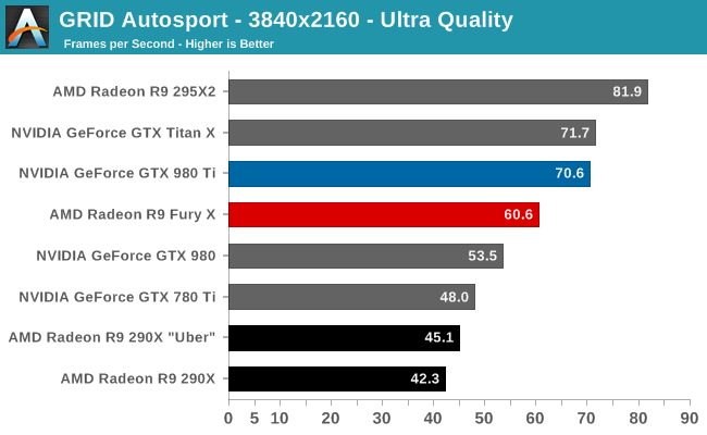
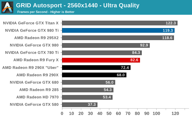
Unfortunately for AMD, after a streak of wins and ties for AMD, things start going off the rails with GRID, very off the rails.
At 4K Ultra this is AMD’s single biggest 4K performance deficit; the card trails the GTX 980 Ti by 14%. The good news is that in the process the card cracks 60fps, so framerates are solid on an absolute basis, though there are still going to be some frames below 60fps for racing purists to contend with.
Where things get really bad is at 1440p, in a situation we have never seen before in a high-end AMD video card review. The R9 Fury X gets pummeled here, trailing the GTX 980 Ti by 30%, and even falling behind the GTX 980 and GTX 780 Ti. The reason it’s getting pummeled is because the R9 Fury X is CPU bottlenecked here; no matter what resolution we pick, the R9 Fury X can’t spit out more than about 82fps here at Ultra quality.
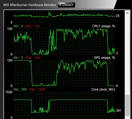
With GPU performance outgrowing CPU performance year after year, this is something that was due to happen sooner or later, and is a big reason that low-level APIs are about to come into the fold. And if it was going to happen anywhere, it would happen with a flagship level video card. Still, with an overclocked Core i7-4960X driving our testbed, this is also one of the most powerful systems available with respect to CPU performance, so AMD’s drivers are burning an incredible amount of CPU time here.
Ultimately GRID serves to cement our concerns about AMD’s performance at 1440p, as it’s very possible that this is the tip of the iceberg. DirectX 11 will go away eventually, but it will still take some time. In the meantime there are a number of 1440p gamers out there, especially with R9 Fury X otherwise being such a good fit for high frame rate 1440p gaming. Perhaps the biggest issue here is that this makes it very hard to justify pairing 1440p 144Hz monitors with AMD’s GPUs, as although 82.6fps is fine for a 60Hz monitor, these CPU issues are making it hard for AMD to deliver framerates more suitable/desirable for those high performance monitors.
Grand Theft Auto V
The final game in our review of the R9 Fury X is our most recent addition, Grand Theft Auto V. The latest edition of Rockstar’s venerable series of open world action games, Grand Theft Auto V was originally released to the last-gen consoles back in 2013. However thanks to a rather significant facelift for the current-gen consoles and PCs, along with the ability to greatly turn up rendering distances and add other features like MSAA and more realistic shadows, the end result is a game that is still among the most stressful of our benchmarks when all of its features are turned up. Furthermore, in a move rather uncharacteristic of most open world action games, Grand Theft Auto also includes a very comprehensive benchmark mode, giving us a great chance to look into the performance of an open world action game.
On a quick note about settings, as Grand Theft Auto V doesn't have pre-defined settings tiers, I want to quickly note what settings we're using. For "Very High" quality we have all of the primary graphics settings turned up to their highest setting, with the exception of grass, which is at its own very high setting. Meanwhile 4x MSAA is enabled for direct views and reflections. This setting also involves turning on some of the advanced redering features - the game's long shadows, high resolution shadows, and high definition flight streaming - but it not increasing the view distance any further.
Otherwise for "High" quality we take the same basic settings but turn off all MSAA, which significantly reduces the GPU rendering and VRAM requirements.
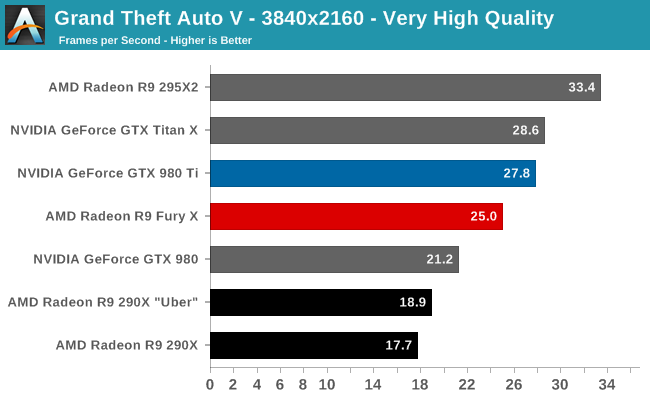
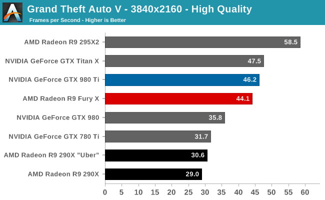
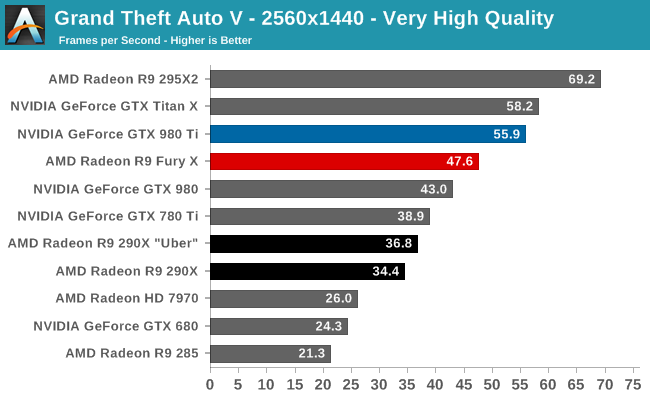
Our final game sees the R9 Fury X go out on either an average or slightly worse than average note, depending on the settings and resolution we are looking at. At our highest 4K settings the R9 Fury X trails the GTX 980 Ti once again, this time by 10%. Worse, at 1440p it’s now 15%. On the other hand if we run at our lower, more playable 4K settings, then the gap is only 5%, roughly in line with the overall average 4K performance gap between the GTX 980 Ti and R9 Fury X.
In this case it’s probably to AMD’s benefit that our highest 4K settings aren’t actually playable on a single GPU card, as the necessary drop in quality gets them closer to NVIDIA’s performance. On the other hand this does reiterate the fact that right now many games will force a tradeoff between resolution and quality if you wish to pursue 4K gaming.
Finally, the performance gains relative to the R9 290X are pretty good. 29% at 1440p, and 44% at the lower quality playable 4K resolution setting.
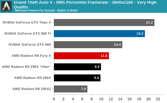
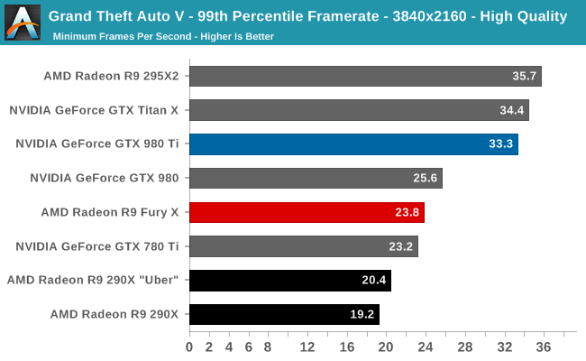
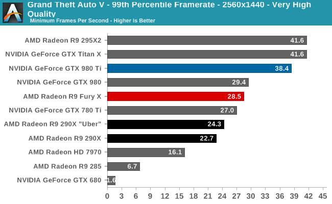
Shifting gears to 99th percentile frametimes however – a much-welcome feature of the game’s built-in benchmark – finds that AMD doesn’t fare nearly as well. At the 99th percentile the R9 Fury X trails the GTX 980 Ti at all times, and significantly so. The deficit is anywhere between 26% at 1440p to 40% at 4K Very High.
What’s happening here is a combination of multiple factors. First and foremost, next to Shadow of Mordor, GTAV is our other VRAM busting game. This, I believe, is why 99th percentile performance dives so hard at 4K Very High for the R9 Fury X, as it only has 4GB of VRAM compared to 6GB on the GTX 980 Ti. But considering where the GTX 980 places – above the R9 Fury X – I also believe there’s more than just VRAM bottlenecking occurring here. The GTX 980 sees at least marginally better framerates with the same size VRAM pool (and a lot less of almost everything else), which leads me to believe that AMD’s drivers may be holding them back here. Certainly the R9 290X comparison lends some possible credit to that, as the 99th percentile gains are under 20%. Regardless, one wouldn’t expect to be VRAM limited at 1440p or 4K without MSAA, especially as this test was not originally designed to bust 4GB cards.
Synthetics
As always we’ll also take a quick look at synthetic performance. Since Fiji is based on the same GCN 1.2 architecture as Tonga (R9 285), we are not expecting too much new here.
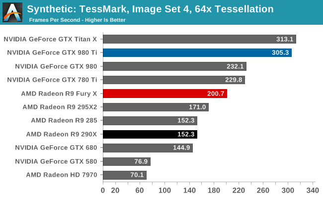
First off we have tessellation performance. As we discussed in greater detail in our look at Fiji’s architecture, AMD has made some tessellation/geometry optimizations in GCN 1.2, and then went above and beyond that for Fiji. As a result tessellation performance on the R9 Fury X is even between than the R9 285 and the R9 290X, improving by about 33% in the case of TessMark. This is the best performing AMD product to date, besting even the R9 295X2. However AMD still won’t quite catch up to NVIDIA for the time being.
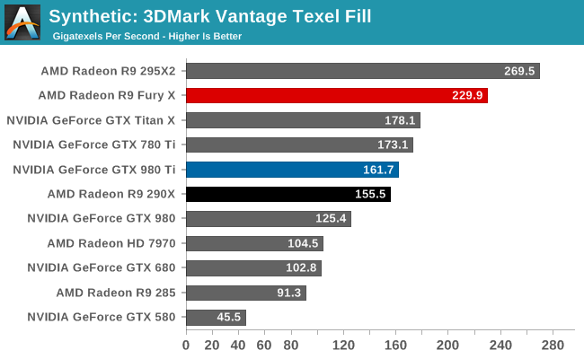
As for texture fillrates, the performance here is outstanding, though not unexpected. R9 Fury X has 256 texture units, the most of any single GPU card, and this increased texture fillrate is exactly in line with the theoretical predictions based on the increased number of texture units.
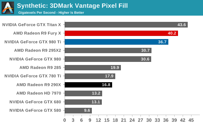
Finally, the 3DMark Vantage pixel fillrate test is not surprising, but it is none the less a solid and important outcome for AMD. Thanks to their delta frame buffer compression technology, they see the same kind of massive pixel fillrate improvements here as we saw on the R9 285 last year, and NVIDIA’s Maxwell 2 series. At this point R9 Fury X’s ROPs are pushing more than 40 billion pixels per second, a better than 2x improvement over the R9 290X despite the identical ROP count, and an important reminder of the potential impact of the combination of compression and HBM’s very high memory bandwidth. AMD’s ROPs are reaching efficiency levels simply not attainable before.
Compute
Shifting gears, we have our look at compute performance. As an FP64 card, the R9 Fury X only offers the bare minimum FP64 performance for a GCN product, so we won’t see anything great here. On the other hand with a theoretical FP32 performance of 8.6 TFLOPs, AMD could really clean house on our more regular FP32 workloads.
Starting us off for our look at compute is LuxMark3.0, the latest version of the official benchmark of LuxRender 2.0. LuxRender’s GPU-accelerated rendering mode is an OpenCL based ray tracer that forms a part of the larger LuxRender suite. Ray tracing has become a stronghold for GPUs in recent years as ray tracing maps well to GPU pipelines, allowing artists to render scenes much more quickly than with CPUs alone.
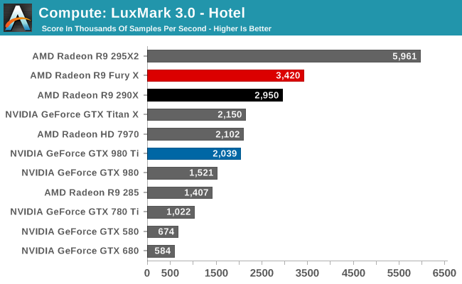
The results with LuxMark ended up being quite a bit of a surprise, and not for a good reason. Compute workloads are shader workloads, and these are workloads that should best illustrate the performance improvements of R9 Fury X over R9 290X. And yet while the R9 Fury X is the fastest single GPU AMD card, it’s only some 16% faster, a far cry from the 50%+ that it should be able to attain.
Right now I have no reason to doubt that the R9 Fury X is capable of utilizing all of its shaders. It just can’t do so very well with LuxMark. Given the fact that the R9 Fury X is first and foremost a gaming card, and OpenCL 1.x traction continues to be low, I am wondering whether we’re seeing a lack of OpenCL driver optimizations for Fiji.
For our second set of compute benchmarks we have CompuBench 1.5, the successor to CLBenchmark. CompuBench offers a wide array of different practical compute workloads, and we’ve decided to focus on face detection, optical flow modeling, and particle simulations.
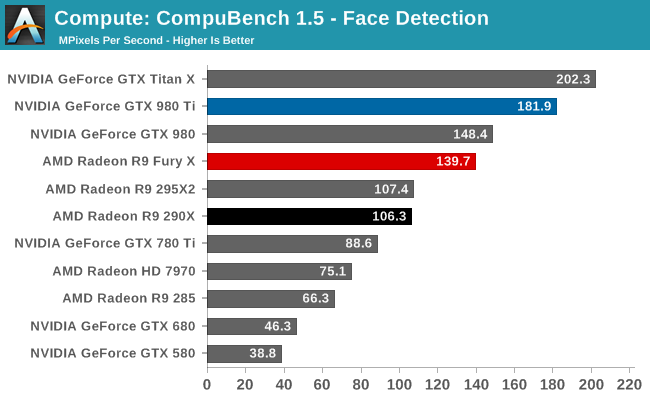
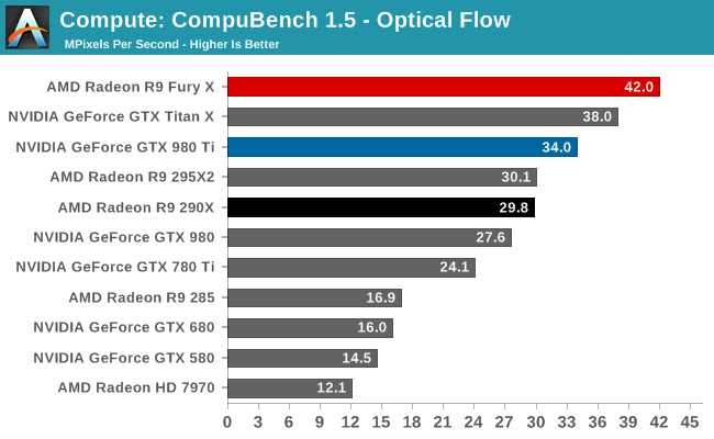
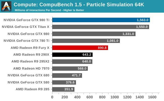
Quickly taking some of the air out of our driver theory, the R9 Fury X’s performance on CompuBench is quite a bit better, and much closer to what we’d expect given the hardware of the R9 Fury X. The Fury X only wins overall at Optical Flow, a somewhat memory-bandwidth heavy test that to no surprise favors AMD’s HBM additions, but otherwise the performance gains across all of these tests are 40-50%. Overall then the outcome over who wins is heavily test dependent, though this is nothing new.
Our 3rd compute benchmark is Sony Vegas Pro 13, an OpenGL and OpenCL video editing and authoring package. Vegas can use GPUs in a few different ways, the primary uses being to accelerate the video effects and compositing process itself, and in the video encoding step. With video encoding being increasingly offloaded to dedicated DSPs these days we’re focusing on the editing and compositing process, rendering to a low CPU overhead format (XDCAM EX). This specific test comes from Sony, and measures how long it takes to render a video.
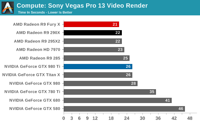
At this point Vegas is becoming increasingly CPU-bound and will be due for replacement. The Fury X none the less shaves off an additional second of rendering time, bringing it down to 21 seconds.
Moving on, our 4th compute benchmark is FAHBench, the official Folding @ Home benchmark. Folding @ Home is the popular Stanford-backed research and distributed computing initiative that has work distributed to millions of volunteer computers over the internet, each of which is responsible for a tiny slice of a protein folding simulation. FAHBench can test both single precision and double precision floating point performance, with single precision being the most useful metric for most consumer cards due to their low double precision performance. Each precision has two modes, explicit and implicit, the difference being whether water atoms are included in the simulation, which adds quite a bit of work and overhead. This is another OpenCL test, utilizing the OpenCL path for FAHCore 17.
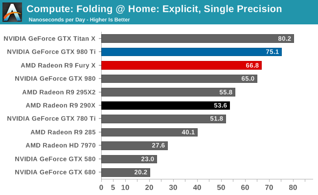
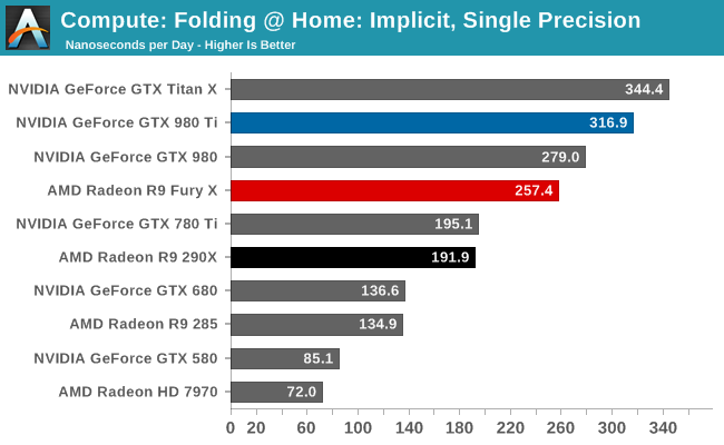
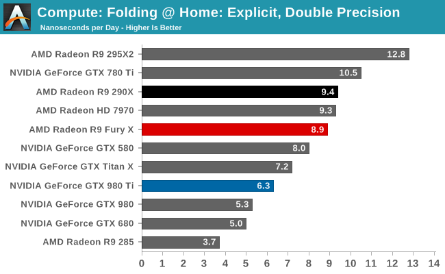
Both of the FP32 tests for FAHBench show smaller than expected performance gains given the fact that the R9 Fury X has such a significant increase in compute resources and memory bandwidth. 25% and 34% respectively are still decent gains, but they’re smaller gains than anything we saw on CompuBench. This does lend a bit more support to our theory about driver optimizations, though FAHBench has not always scaled well with compute resources to begin with.
Meanwhile FP64 performance dives as expected. With a 1/16 rate it’s not nearly as bad as the GTX 900 series, but even the Radeon HD 7970 is beating the R9 Fury X here.
Wrapping things up, our final compute benchmark is an in-house project developed by our very own Dr. Ian Cutress. SystemCompute is our first C++ AMP benchmark, utilizing Microsoft’s simple C++ extensions to allow the easy use of GPU computing in C++ programs. SystemCompute in turn is a collection of benchmarks for several different fundamental compute algorithms, with the final score represented in points. DirectCompute is the compute backend for C++ AMP on Windows, so this forms our other DirectCompute test.
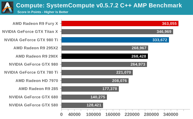
Our C++ AMP benchmark is another case of decent, though not amazing, GPU compute performance gains. The R9 Fury X picks up 35% over the R9 290X. And in fact this is enough to vault it over NVIDIA’s cards to retake the top spot here, though not by a great amount.
Power, Temperature, & Noise
As always, last but not least is our look at power, temperature, and noise. Next to price and performance of course, these are some of the most important aspects of a GPU, due in large part to the impact of noise. All things considered, a loud card is undesirable unless there’s a sufficiently good reason – or sufficiently good performance – to ignore the noise.
Starting with voltages, at least for the time being we have nothing to report on R9 Fury X as far as voltages go. AMD is either not exposing voltages in their drivers, or our existing tools (e.g. MSI Afterburner) do not know how to read the data, and as a result we cannot see any of the voltage information at this time.
| Radeon R9 Fury X Average Clockspees | ||
| Game | R9 Fury X | |
| Max Boost Clock | 1050MHz | |
| Battlefield 4 |
1050MHz
|
|
| Crysis 3 |
1050MHz
|
|
| Mordor |
1050MHz
|
|
| Civilization: BE |
1050MHz
|
|
| Dragon Age |
1050MHz
|
|
| Talos Principle |
1050MHz
|
|
| Far Cry 4 |
1050MHz
|
|
| Total War: Attila |
1050MHz
|
|
| GRID Autosport |
1050MHz
|
|
| Grand Theft Auto V |
1050MHz
|
|
| FurMark |
985MHz
|
|
Jumping straight to average clockspeeds then, with an oversized cooler and a great deal of power headroom, the R9 Fury X has no trouble hitting and sustaining its 1050MHz boost clockspeed throughout every second of our benchmark runs. The card was designed to be the pinnacle of Fiji cards, and ensuring it always runs at a high clockspeed is one of the elements in doing so. The lack of throttling means there’s really little to talk about here, but it sure gets results.
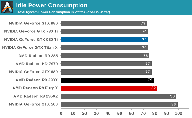
Idle power does not start things off especially well for the R9 Fury X, though it’s not too poor either. The 82W at the wall is a distinct increase over NVIDIA’s latest cards, and even the R9 290X. On the other hand the R9 Fury X has to run a CLLC rather than simple fans. Further complicating factors is the fact that the card idles at 300MHz for the core, but the memory doesn’t idle at all. HBM is meant to have rather low power consumption under load versus GDDR5, but one wonders just how that compares at idle.
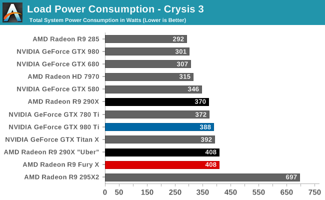
Switching to load power consumption, we go first with Crysis 3, our gaming load test. Earlier in this article we discussed all of the steps AMD took to rein in on power consumption, and the payoff is seen here. Equipped with an R9 Fury X, our system pulls 408W at the wall, a significant amount of power, but only 20W at the wall more than the same system with a GTX 980 Ti. Given that the R9 Fury X’s framerates trail the GTX 980 Ti here, this puts AMD’s overall energy efficiency in a less-than-ideal spot, but it’s not poor either, especially compared to the R9 290X. Power consumption has essentially stayed put while performance has gone up 35%+.
On a side note, as we mentioned in our architectural breakdown, the amount of power this card draws will depend on its temperature. 408W at the wall at 65C is only 388W at the wall at 40C, as current leakage scales with GPU temperature. Ultimately the R9 Fury X will trend towards 65C, but it means that early readings can be a bit misleading.
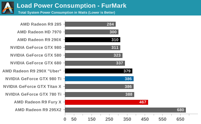
As for FurMark, what we find is that power consumption at the wall is much higher, which far be it from being a problem for AMD, proves that the R9 Fury X has much greater thermal and electrical limits than the R9 290X, or the NVIDIA completion for that matter. AMD ultimately does throttle the R9 Fury X here, at around 985MHz, but the card easily draws quite a bit of power and dissipates quite a bit of heat in the process. If the card had a gaming scenario that called for greater power consumption – say BIOS modded overclocking – then these results paint a favorable picture.
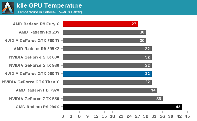
Moving on to temperatures, the R9 Fury X starts off looking very good. Even at minimum speeds the pump and radiator leads to the Fiji GPU idling at just 27C, cooler than anything else on this chart. More impressive still is the R9 290X comparison, where the R9 Fury X is some 15C cooler, and this is just at idle.
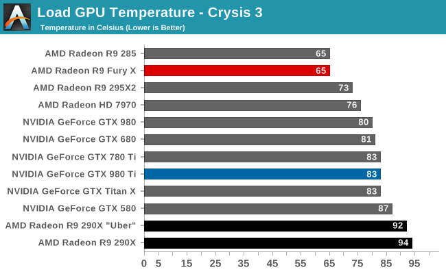
Loading up a game, after a good 10 minutes or so the R9 Fury X finally reaches its equilibrium temperature of 65C. Though the default target GPU temperature is 75C, it’s at 65C that the card finally begins to ramp up the fan in order to increase cooling performance. The end result is that the card reaches equilibrium at this point and in our experience should not exceed this temperature.
Compared to the NVIDIA cards, this is an 18C advantage in AMD’s favor. GPU temperatures are not everything – ultimately it’s fan speed and noise we’re more interested in – but for AMD GPU temperatures are an important component of controlling GPU power consumption. By keeping the Fiji GPU at 65C AMD is able to keep leakage power down, and therefore energy efficiency up. R9 Fury X would undoubtedly fare worse in this respect if it got much warmer.
Finally, it’s once again remarkable to compare the R9 Fury X to the R9 290X. With the former AMD has gone cool to keep power down, whereas with the latter AMD went hot to improve cooling efficiency. As a result the R9 Fury X is some 29C cooler than the R9 290. One can only imagine what that has done for leakage.
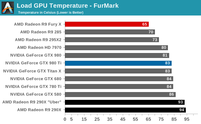
The situation is more or less the same under FurMark. The NVIDIA cards are set to cap at 83C, and the R9 Fury X is set to cap at 65C. This is regardless of whether it’s a game or a power virus like FurMark.
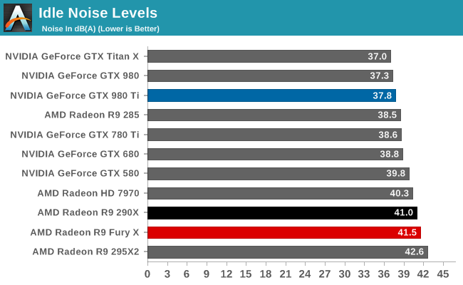
Last but not least, we have noise. Starting with idle noise, as we mentioned in our look at the build quality of the R9 Fury X, the card’s cooler is effective under load, but a bit of a liability at idle. The use of a pump brings with it pump noise, and this drives up idle noise levels by around 4dB. 41.5dB is not too terrible for a closed case, and it’s not an insufferable noise, but HTPC users will want to be weary. This if anything makes a good argument for looking forward to the R9 Nano.
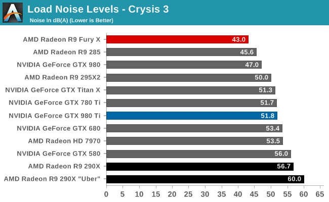
Because the R9 Fury X starts out a bit loud due to pump noise, the actual noise increase under load is absolutely miniscule. The card tops out at 19% fan speed, 4% (or about 100 RPM) over its default fan speed of 15%. As a result we measure an amazing 43dB under load. For a high performance video card. For a high performance card within spitting distance of NVIDIA’s flagship and one of the best air cooled video cards of all time.
These results admittedly were not unexpected – one need only look at the R9 295X2 to get an idea of what a CLLC could do for noise – but they are none the less extremely impressive. Most midrange cards are louder than this despite offering a fraction of the R9 Fury X’s gaming performance, which puts the R9 Fury X at a whole new level for load noise from a high performance video card.
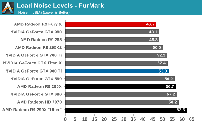
The trend continues under FurMark. The fan speed ramps up quite a bit further here thanks to the immense load from FurMark, but the R9 Fury X still perseveres. 46.7 dB(A) is once again better than a number of mid-range video cards, never mind the other high-end cards in this roundup. The R9 Fury X is dissipating 330W of heat and yet it’s quieter than the GTX 980 at half that heat, and around 6 dB(A) quieter than the 250W GM200 cards.
There really isn’t enough nice things I can say about the R9 Fury X’s cooler. AMD took the complaints about the R9 290 series to heart, and produced something that wasn’t just better than their previous attempt, but a complete inverse of their earlier strategy. The end result is that the R9 Fury X is well near whisper quiet under gaming, and only a bit louder under even the worst case scenario. This is a remarkable change, and one that ears everywhere will appreciate.
That said, the mediocre idle noise showing will undoubtedly dog the R9 Fury X in some situations. For most cases it will not be an issue, but it does close some doors on ultra-quiet setups. The R9 Fury X in that respect is merely very, very quiet.
Overclocking
Finally, no review of a high-end video card would be complete without a look at overclocking performance.
To get right to the point here, overclockers looking at out of the box overclocking performance are going to come away disappointed. While cooling and power delivery are overbuilt, in other respects the R9 Fury X is very locked down when it comes to overclocking. There is no voltage control at this time (even unofficial), there is no official HBM clockspeed control, and the card’s voltage profile has been finely tuned to avoid needing to supply the card with more voltage than is necessary. As a result the card has relatively little overclocking potential without voltage adjustments.
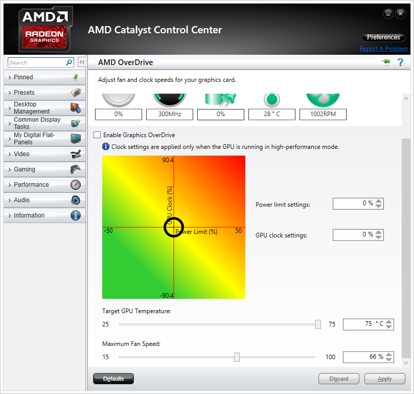
So what do we get for overclocking?
| Radeon R9 Fury X Overclocking | ||||
| Stock | Overclocked | |||
| Boost Clock | 1050Mhz | 1125MHz | ||
| Memory Clock | 1Gbps (500MHz DDR) | 1Gbps (500MHz DDR) | ||
| Max Voltage | N/A | N/A | ||
Our efforts net us 75MHz, which is actually 25MHz less than what AMD published in their reviewer’s guide. Even 100MHz would lead to artifacting in some games, requiring that we step down to a 75MHz overclock to have a safe and sustainable overclock.
The end result is that the overclocked R9 Fury X runs at 1125MHz core and 1Gbps memory, a 75MHz (7%) increase in the GPU clockspeed and 0% increase in the memory clockspeed. This puts a very narrow window on expected performance gains, as we shouldn’t exceed a 7% gain in any game, and will almost certainly come in below 7% in most games.
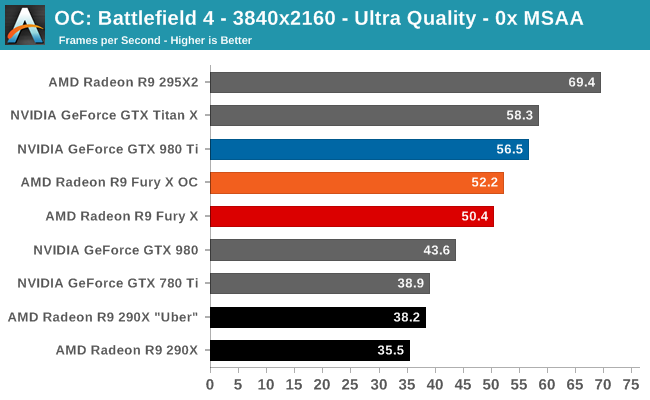
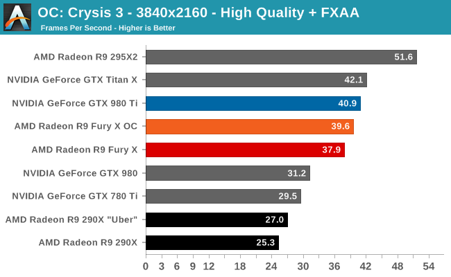
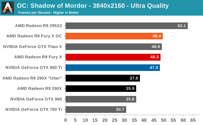
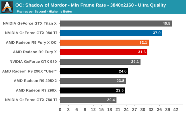
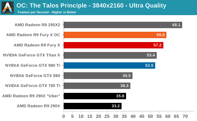
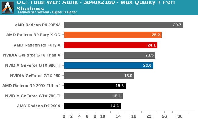
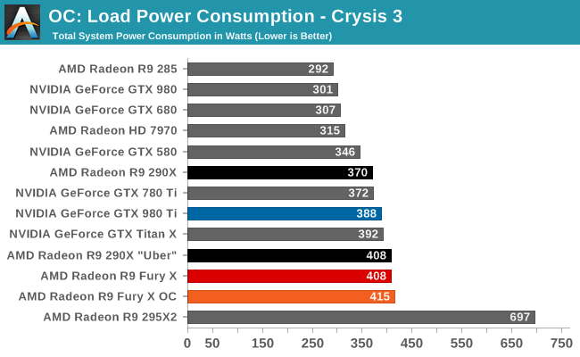
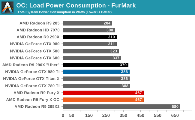
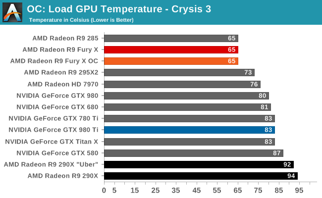
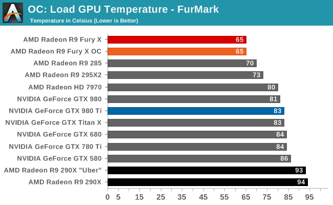
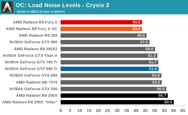
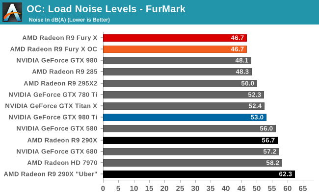
Our gaming benchmarks find just that. A few percent performance improvement there, a 5% improvement there. Overall we wouldn’t go as far as saying there no reason to overclock, but with such limited gains it’s hardly worth the trouble right now.
True overclocking is going to have to involve BIOS modding, a riskier and warranty-voiding strategy, but one that should be far more rewarding. With more voltage I have little doubt that R9 Fury X could clock higher, though it’s impossible to guess by how much at this time. In any case the card is certainly built for it, as the oversized cooler, high power delivery capabilities, and dual BIOS switch provide all the components necessary for such an overclocking attempt.
Meanwhile HBM is a completely different bag, and while unofficial overclocking is looking promising, as a new technology it will take some time to get a good feel for it and understand just what kind of performance improvements it can deliver. The R9 Fury X is starting out with quite a bit of memory bandwidth right off the bat (512GB/sec), so it may not be bandwidth starved as often as other cards like the R9 290X was.
Final Words
Bringing this review to a close, AMD has certainly thrown a great deal at us with the Radeon R9 Fury X. After the company’s stumble with their last single-GPU flagship, the Radeon R9 290X, they have reevaluated what they want to do, how they want to build their cards, and what kind of performance they want to aim for. As a result the R9 Fury X is an immensely interesting card.
From a technical perspective AMD has done a ton right here. The build quality is excellent, the load acoustic performance is unrivaled, the performance is great. Meanwhile although the ultimate value of High Bandwidth Memory to the buyer is only as great as the card’s performance, from a hobbyist perspective I am excited for what it means for future cards. The massive bandwidth improvements, the power savings, and the space savings have all done wonderful things for the R9 Fury X, and will do so for other cards in the future as well.
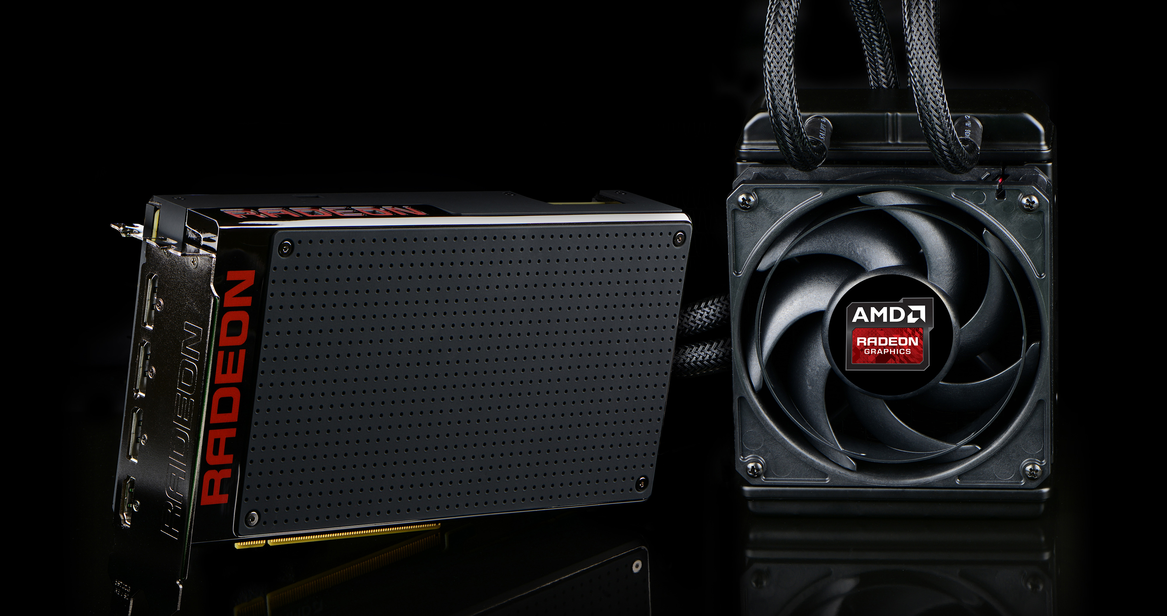
Compared to the R9 290X then, AMD has gone and done virtually everything they have needed to do in order to right what was wrong, and to compete with an NVIDIA energized by GTX Titan and the Maxwell architecture. As self-admittedly one of the harshest critics of the R9 290X and R9 290 due to the 290 series’ poor reference acoustic performance, I believe AMD has built an amazing card with the R9 Fury X. I dare say AMD finally “gets it” on card quality and so much more.
Had this card launched against the GTX Titan X a couple of months ago, where we would be today is talking about how AMD doesn’t quite dethrone the NVIDIA flagship, but instead how they serve as a massive spoiler, delivering so much of GTX Titan X’s performance for a fraction of the cost. But, unfortunately for AMD, this is not what has happened. The competition for the R9 Fury X is not an overpriced GTX Titan X, but a well-priced GTX 980 Ti, which to add insult to injury launched first, even though it was in all likelihood NVIDIA’s reaction to R9 Fury X.
The problem for AMD is that the R9 Fury X is only 90% of the way there, and without a price spoiler effect the R9 Fury X doesn’t go quite far enough. At 4K it trails the GTX 980 Ti by 4%, which is to say that AMD could not manage a strict tie or to take the lead. To be fair to AMD, a 4% difference in absolute terms is unlikely to matter in the long run, and for most practical purposes the R9 Fury X is a viable alternative to the GTX 980 Ti at 4K. None the less it does technically trail the GTX 980 Ti here, and that’s not the only issue that dogs such a capable card.
At 2560x1440 the card loses its status as a viable alternative. AMD’s performance deficit is over 10% at this point, and as we’ve seen in a couple of our games, AMD is hitting some very real CPU bottlenecking even on our high-end system. Absolute framerates are high enough that this only occurs at lower resolutions thanks to the high framerates these resolutions afford (and not a problem for 60Hz monitors), however at the same time AMD is also promoting 2560x1440@144Hz Freesync monitors, which these CPU bottlenecking issues greatly undercut.
The bigger issue, I suppose, is that while the R9 Fury X is very fast, I don’t feel we’ve reached the point where 4K gaming on a single GPU is the best way to go; too often we still need to cut back on image quality to reach playable framerates. 4K is arguably still the domain of multi-GPU setups, meanwhile cards like the R9 Fury X and GTX 980 Ti are excellent cards for 2560x1440 gaming, or even 1080p gaming for owners who want to take advantage of the image quality improvements from Virtual Super Resolution.
The last issue that dogs AMD here is VRAM capacity. At the end of the day first-generation HBM limits them to 4GB of VRAM, and while they’ve made a solid effort to work around the problem, there is only so much they can do. 4GB is enough right now, but I am concerned that R9 Fury X owners will run into VRAM capacity issues before the card is due for a replacement even under an accelerated 2 year replacement schedule.
Once you get to a straight-up comparison, the problem AMD faces is that the GTX 980 Ti is the safer bet. On average it performs better at every resolution, it has more VRAM, it consumes a bit less power, and NVIDIA’s drivers are lean enough that we aren’t seeing CPU bottlenecking that would impact owners of 144Hz displays. To that end the R9 Fury X is by no means a bad card – in fact it’s quite a good card – but NVIDIA struck first and struck with a slightly better card, and this is the situation AMD must face. At the end of the day one could do just fine with the R9 Fury X, it’s just not what I believe to be the best card at $649.
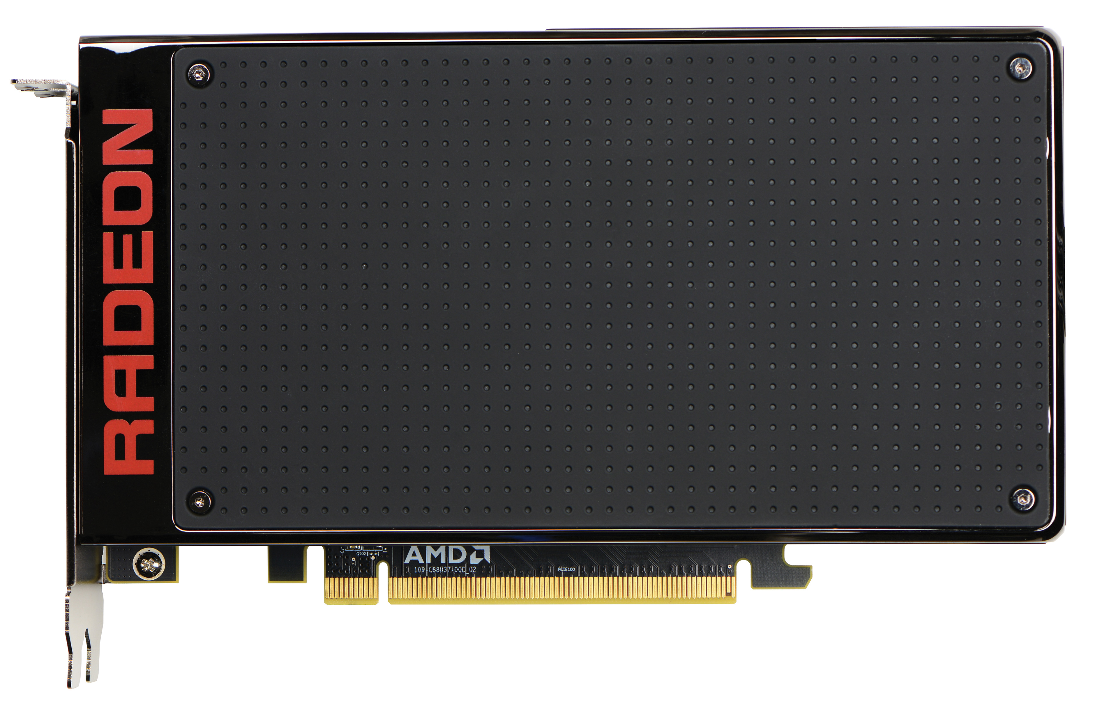
With that said, the R9 Fury X does have some advantages, that at least in comparing reference cards to reference cards, NVIDIA cannot touch, and these advantages give the R9 Fury X a great niche to reside in. The acoustic performance is absolutely amazing, and while it’s not enough to overcome some of the card’s other issues overall, if you absolutely must have the lowest load noise possible from a reference card, the R9 Fury X should easily impress you. I doubt that even the forthcoming R9 Nano can match what AMD has done with the R9 Fury X in this respect. Meanwhile, although the radiator does present its own challenges, the smaller size of the card should be a boon to small system builders who need something a bit different than standard 10.5” cards. Throw a couple of these into a Micro-ATX SFF PC, and it will be the PSU, not the video cards, that become your biggest concern.
Ultimately I believe AMD deserves every bit of credit they get for the R9 Fury X. They have put together a solid card that shows an impressive improvement over what they gave us 2 years ago with R9 290X. With that said, as someone who would like to see AMD succeed and prosper, the fact that they get so close only to be outmaneuvered by NVIDIA once again makes the current situation all the more painful; it’s one thing to lose to NVIDIA by feet, but to lose by inches only reminds you of just how close they got, how they almost upset NVIDIA. At the end of the day I think AMD can at least take home credit for forcing the GTX 980 Ti in to existence, which has benefitted the wider hobbyist community. Still, looking at AMD’s situation I can’t help but wonder what happens from here, as it seems like AMD badly needed a win they won’t quite get.
Finally, with the launch of the R9 Fury X behind us, it’s time to turn our gaze towards the future, the very near future. The R9 Fury X’s younger sibling, the R9 Fury, launches in 2 weeks. Though certainly slower by virtue of its cut-down Fiji GPU, it is also $100 cheaper, and is a more traditional air-cooled card design as well. With NVIDIA still selling the 4GB GTX 980 for $500, the playing field is going to be much different below the R9 Fury X, so I am curious to see just how things shape up on the 14th.


